TPS65163
SLVSA28 –OCTOBER 2009
www.ti.com
VIN
R
Short-Circuit
Mode
R
-
FBB
FBN
300μA
1.65V
+
Short-Circuit
Comparator
Control
Logic
Normal
Mode
+
-
2.5mA
Error
Amplifier
CTRLN
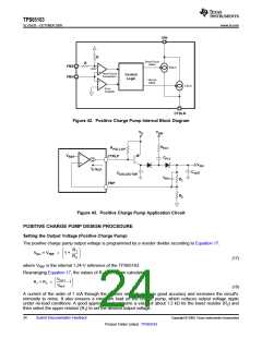
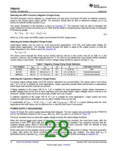
Figure 42. Positive Charge Pump Internal Block Diagram
V
V
S
SW
R
R
FLY
C
PULL-UP
-
V
CTRLP
REF
FLY
+
V
GH
I
CTRLP
C
C
OUT
COLLECTOR
C
FF
R
R
1
2
FBP
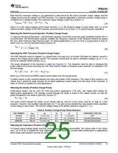
Figure 43. Positive Charge Pump Application Circuit
POSITIVE CHARGE PUMP DESIGN PROCEDURE
Setting the Output Voltage (Positive Charge Pump)
The positive charge pump output voltage is programmed by a resistor divider according to Equation 17.
æ
ç
è
R1 ö
VGH = VREF
´
1 +
÷
R2 ø
(17)
(18)
where VREF is the internal 1.24-V reference of the TPS65163.
Rearranging Equation 17, the values of R1 and R2 are calculated:
æ VOUT
ö
÷
ø
R1 = R2
´
-1
ç
VREF
è
A current of the order of 1 mA through the resistor network ensures good accuracy and increases the circuit's
immunity to noise. It also ensures a minimum load on the charge pump, which reduces output voltage ripple
under no-load conditions. A good approach is to assume a value of about 1.2 kΩ for the lower resistor (R2) and
then select the upper resistor (R1) to set the desired output voltage.
24
Submit Documentation Feedback
Copyright © 2009, Texas Instruments Incorporated
Product Folder Link(s) :TPS65163

 TI [ TEXAS INSTRUMENTS ]