TPS65163
www.ti.com
SLVSA28 –OCTOBER 2009
CDLY ´ VREF
tDLY
=
IDLY
(29)
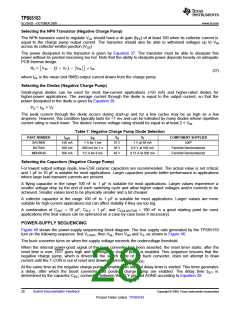
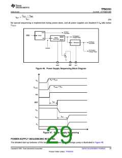
No special sequencing is implemented during power-down, and all power supplies are disabled if VIN falls below
VUVLO
.
To Buck
Converter
OUT
PG
UVLO
EN Buck
To Negative
Charge Pump
RESET
RESET
Reset
Generator
IN
To Boost
Converter
Delay
IN
OUT
Latched
To Positive
Charge Pump
CRST
RST
DLY
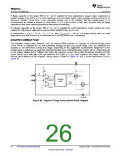
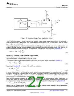
Figure 46. Power Supply Sequencing Block Diagram
VIN > VUVLO
VIN
VLOGIC > VPG
VLOGIC
PG
tRST
RST
VGL
VGH
VS
tDLY
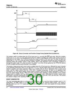
Figure 47. Power Supply Sequencing
POWER-SUPPLY SEQUENCING IN DETAIL
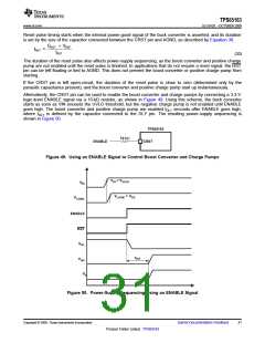
The detailed start-up behavior of the boost converter and positive charge pump is illustrated in Figure 48.
Copyright © 2009, Texas Instruments Incorporated
Submit Documentation Feedback
29
Product Folder Link(s) :TPS65163

 TI [ TEXAS INSTRUMENTS ]