TPS65163
www.ti.com
SLVSA28 –OCTOBER 2009
Note that the maximum voltage in an application is determined by the boost converter output voltage and the
voltage drop across the diodes and PNP transistor. For a typical application in which the positive charge pump is
configured as a voltage doubler, the maximum output voltage is given by Equation 19.
VGH(MAX) = 2 ´ V
(
-
2 × V
- VCE
)
(
)
S
F
(19)
where VS is the output voltage of the boost converter, VF is the forward voltage of each diode, and VCE is the
collector-emitter voltage of the PNP transistor (recommended to be at least 1 V to avoid transistor saturation).
Selecting the Feed-Forward Capacitor (Positive Charge Pump)
To improve transient performance, a feed-forward capacitor connected across the upper feedback resistor (R1) is
recommended. The feed-forward capacitor modifies the frequency response of the feedback network by adding
the zero, which improves high frequency gain. For typical applications, a zero at 5 kHz is a good place to start, in
which case CFF can be calculated using Equation 20.
1
CFF
=
2 ´ p ´ 5 kHz ´ R1
(20)
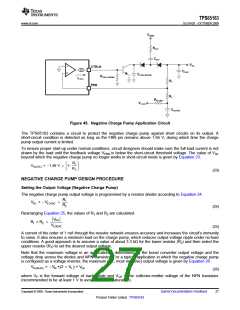
Selecting the PNP Transistor (Positive Charge Pump)
The PNP transistor used to regulate VGH should have a dc gain (hFE) of at least 100 when its collector current is
equal to the charge pump output current. The transistor should also be able to withstand voltages up to 2 × VS
across its collector-emitter junction (VCE).
The power dissipated in the transistor is given by Equation 21. The transistor must be able to dissipate this
power without its junction becoming too hot. Note that the ability to dissipate power depends on adequate PCB
thermal design.
é
ù
- VGH ´ IGH
PQ
=
2 ´ V
-
2 ´ V
(
)
(
)
S
F
ë
û
(21)
where IGH is the mean (not RMS) output current drawn from the charge pump.
A pullup resistor is also required between the base and emitter of the transistor. The value of this resistor is not
critical, but it should be large enough not to divert significant current away from the base of the transistor. A
value of 100 kΩ is suitable for most applications.
Selecting the Diodes (Positive Charge Pump)
Small-signal diodes can be used for most low-current applications (<50 mA), and higher-rated diodes for
higher-power applications. The average current through the diode is equal to the output current, so that the
power dissipated in the diode is given by Equation 22.
P = IGH ´ VF
D
(22)
The peak current through the diode occurs during start-up, and for a few cycles may be as high as a few
amperes. However, this condition typically lasts for <1 ms and can be tolerated by many diodes whose repetitive
current rating is much lower. The reverse voltage rating of the diodes should be equal to 2 × VS.
Table 6. Positive Charge-Pump Diode Selection
PART NUMBER
BAV99W
IAVG
IPK
VR
VF
COMPONENT SUPPLIER
NXP
150 mA
200 mA
500 mA
1 A for 1 ms
600 mA for 1 s
5.5 A for 8 ms
75 V
30 V
40 V
1 V at 50 mA
0.8 V at 100 mA
0.51 at 500 mA
BAT54S
Fairchild Semiconductor
Fairchild Semiconductor
MBR0540
Selecting the Capacitors (Positive Charge Pump)
For lowest output voltage ripple, low-ESR ceramic capacitors are recommended. The actual value is not critical,
and 1 µF to 10 µF is suitable for most applications. Larger capacitors provide better performance in applications
where large load transient currents are present.
Copyright © 2009, Texas Instruments Incorporated
Submit Documentation Feedback
25
Product Folder Link(s) :TPS65163

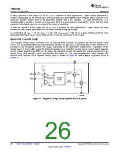
 TI [ TEXAS INSTRUMENTS ]