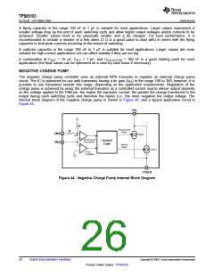
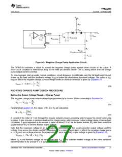
TPS65163
SLVSA28 –OCTOBER 2009
www.ti.com
tDLY
RST
≈1ms
GD
VS
≈VIN
VS
VSW
VFBP
VGH
VIN
1.24V
100mV
TIME
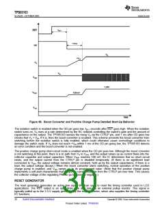
Figure 48. Boost Converter and Positive Charge Pump Detailed Start-Up Behavior
The isolation switch is enabled when the GD pin goes low, tDLY seconds after RST goes high. When the isolation
switch turns on, VS rises at a rate determined by the RC network controlling the switch's gate and the amount of
capacitance on the output. The TPS65163 senses the rising VS via the CTRLP pin, and 1 ms after GD goes low
checks that VS ≈ VIN. If it is, then the boost converter is enabled. This scheme prevents the boost converter from
switching before the isolation switch is fully enabled, which could otherwise cause overvoltage conditions to
damage the switch node. If VS does not reach ≈VIN within 1 ms of the GD pin going low, the TPS65163 detects
an error condition and the boost converter is not enabled.
The positive charge pump short-circuit mode is enabled when the GD pin goes low. Although the boost converter
is not switching at this point, there is a dc path from VS to VGH, and the output ramps up as current flows into the
collector capacitor and output capacitors. When VFBP reaches 100 mV, the IC determines that no short circuit
exists, and the output current from the CTRLP pin is disabled temporarily. (If there is no significant load
connected to VGH, the output voltage remains almost constant, held up by the output capacitance; if there is a
load, the output voltage decays.) When the boost converter starts switching, normal operation of the positive
charge pump is enabled, and VGH ramps up to its programmed value. (Note that the positive charge pump
implements a soft-start characteristic that ramps the current available from the CTRLP pin over time. This causes
the collector voltage of the regulating PNP to go temporarily negative.)
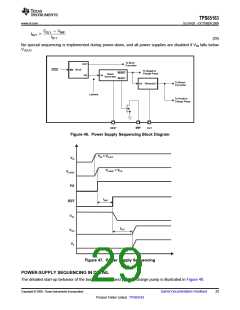
RESET GENERATOR
The reset generator generates an active low signal that can used to reset the timing controller used in LCD
applications. The RST output is an open-drain type and requires an external pullup resistor. This signal is
typically pulled up to the 3.3-V supply generated by the buck converter, which also supplies the timing controller
I/O functions.
30
Submit Documentation Feedback
Copyright © 2009, Texas Instruments Incorporated
Product Folder Link(s) :TPS65163

 TI [ TEXAS INSTRUMENTS ]