TPS65163
SLVSA28 –OCTOBER 2009
www.ti.com
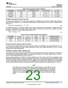
A flying capacitor in the range 100 nF to 1 µF is suitable for most applications. Larger values experience a
smaller voltage drop by the end of each switching cycle and allow higher output voltages and/or currents to be
achieved. Smaller values tend to be physically smaller and a bit cheaper. For best performance, it is
recommended to include a resistor of a few ohms (2 Ω is a good value to start with) in series with the flying
capacitor to limit peak currents occurring at the instant of switching.
A collector capacitor in the range 100 nF to 1 µF is suitable for most applications. Larger values are more
suitable for high-current applications but can affect stability if they are too big.
A combination of COUT = 10 µF, CFLY = 1 µF, and CCOLLECTOR = 100 nF is a good starting point for most
applications (the final values can be optimized on a case-by-case basis if necessary).
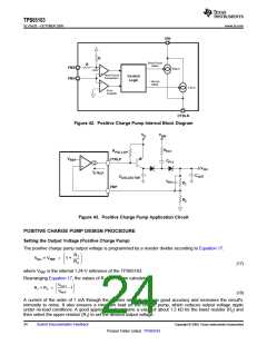
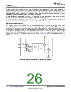
NEGATIVE CHARGE PUMP
The negative charge pump controller uses an external NPN transistor to regulate an external charge pump
circuit. The IC is optimized for use with transistors having a dc gain (hFE) in the range 100 to 300; however, it is
possible to use transistors outside this range, depending on the application requirements. Regulation of the
charge pump is achieved by using the external transistor as a controlled current source whose output depends
on the voltage applied to the FBN pin: the higher the transistor current, the greater the charge transferred to the
output during each switching cycle and therefore the higher (i.e., the more negative) the output voltage. The
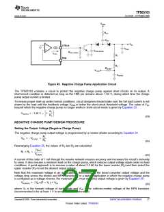
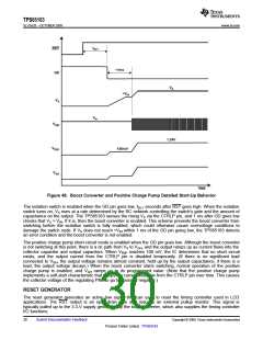
internal block diagram of the negative charge pump is shown in Figure 44, and a typical application circuit in
Figure 45.
VIN
R
Short-Circuit
Mode
R
-
FBB
FBN
300μA
1.65V
+
Short-Circuit
Comparator
Control
Logic
Normal
Mode
+
-
2.5mA
Error
Amplifier
CTRLN
Figure 44. Negative Charge Pump Internal Block Diagram
26
Submit Documentation Feedback
Copyright © 2009, Texas Instruments Incorporated
Product Folder Link(s) :TPS65163

 TI [ TEXAS INSTRUMENTS ]