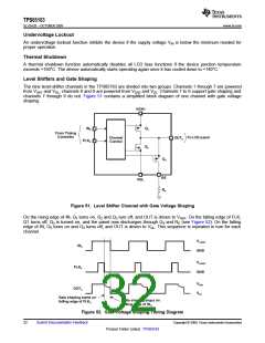
TPS65163
SLVSA28 –OCTOBER 2009
www.ti.com
Selecting the NPN Transistor (Negative Charge Pump)
The NPN transistor used to regulate VGL should have a dc gain (hFE) of at least 100 when its collector current is
equal to the charge pump output current. The transistor should also be able to withstand voltages up to VIN
across its collector-emitter junction (VCE).
The power dissipated in the transistor is given by Equation 27. The transistor must be able to dissipate this
power without its junction becoming too hot. Note that the ability to dissipate power depends heavily on adequate
PCB thermal design.
é
ù
- VGL ´ IGL
PQ
=
V IN
-
2 ´ V
(
)
F
ë
û
(27)
where IGL is the mean (not RMS) output current drawn from the charge pump.
Selecting the Diodes (Negative Charge Pump)
Small-signal diodes can be used for most low-current applications (<50 mA) and higher-rated diodes for
higher-power applications. The average current through the diode is equal to the output current, so that the
power dissipated in the diode is given by Equation 28.
PD = IGL × VF
The peak current through the diode occurs during start-up and for a few cycles may be as high as a few
amperes. However, this condition typically lasts for <1 ms and can be tolerated by many diodes whose repetitive
current rating is much lower. The diodes' reverse voltage rating should be equal to at least 2 × VIN.
Table 7. Negative Charge Pump Diode Selection
PART NUMBER
BAV99W
IAVG
IPK
VR
VF
COMPONENT SUPPLIER
NXP
150 mA
200 mA
500 mA
1 A for 1 ms
600 mA for 1 s
5.5 A for 8 ms
75 V
30 V
40 V
1 V at 50 mA
0.8 V at 100 mA
0.51 A at 500 mA
BAT54S
Fairchild Semiconductor
Fairchild Semiconductor
MBR0540
Selecting the Capacitors (Negative Charge Pump)
For lowest output voltage ripple, low-ESR ceramic capacitors are recommended. The actual value is not critical,
and 1 µF to 10 µF is suitable for most applications. Larger capacitors provide better performance in applications
where large load transient currents are present.
A flying capacitor in the range 100 nF to 1 µF is suitable for most applications. Larger values experience a
smaller voltage drop by the end of each switching cycle and allow higher output voltages and/or currents to be
achieved. Smaller values tend to be physically smaller and a bit cheaper.
A collector capacitor in the range 100 nF to 1 µF is suitable for most applications. Larger values are more
suitable for high-current applications but can affect stability if they are too big.
A combination of COUT = 10 µF, CFLY = 1 µF, and CCOLLECTOR = 100 nF is a good starting point for most
applications (the final values can be optimized on a case-by-case basis if necessary).
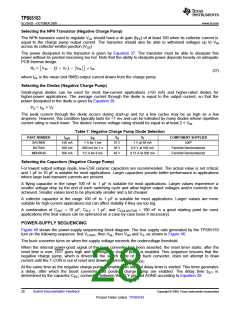
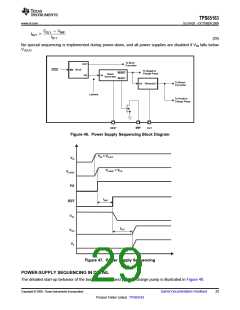
POWER-SUPPLY SEQUENCING
Figure 46 shows the power-supply sequencing block diagram. The four supply rails generated by the TPS65163
turn on the following sequence: first VLOGIC, then VGL, then VGH and VS, as shown in Figure 46.
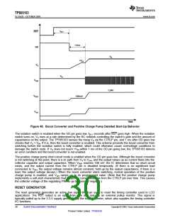
The buck converter turns on when the supply voltage exceeds the undervoltage threshold.
When the internal power-good signal of the buck converter has been asserted, the reset timer starts; after the
reset time is over, RST goes high and the negative charge pump is enabled. This sequence ensures that the
negative charge pump, which is driven by the switch node of the buck converter, does not attempt to draw
current until the T-CON is out of reset and drawing current from VLOGIC
.
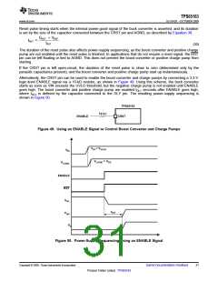
At the same time as the negative charge pump is enabled, an internal delay timer is started. This timer generates
a delay, after which the boost converter and positive charge pump are enabled. The delay time tDLY is
determined by the capacitor CDLY connected between the DLY pin and AGND according to Equation 29.
28
Submit Documentation Feedback
Copyright © 2009, Texas Instruments Incorporated
Product Folder Link(s) :TPS65163

 TI [ TEXAS INSTRUMENTS ]