TPS54531
www.ti.com
SLVSBI5 –MAY 2013
Where ΔIout is the change in output current, Fsw is the regulators switching frequency and ΔVout is the
allowable change in the output voltage. For this example, the transient load response is specified as a 5%
change in Vout for a load step of 2.5 A. For this example, ΔIout = 2.5 A and ΔVout = 0.05 x 5.0 = 0.250 V. Using
these numbers gives a minimum capacitance of 35 μF. This value does not take the ESR of the output capacitor
into account in the output voltage change. For ceramic capacitors, the ESR is usually small enough to ignore in
this calculation.
Equation 12 calculates the minimum output capacitance needed to meet the output voltage ripple specification.
Where fsw is the switching frequency, Voripple is the maximum allowable output voltage ripple, and Iripple is the
inductor ripple current. In this case, the maximum output voltage ripple is 30 mV. Under this requirement
Equation 12, yields 14 µF.
1
1
Co >
×
Voripple
Iripple
8× f sw
(12)
Equation 13 calculates the maximum ESR an output capacitor can have to meet the output voltage ripple
specification. Equation 13 indicates the ESR should be less than 15.6 mΩ. In this case, the ceramic caps’ ESR is
much smaller than 15.6 mΩ.
Voripple
Resr <
Iripple
(13)
Additional capacitance de-ratings for aging, temperature and DC bias should be factored in which increases this
minimum value. For this example, two 47 μF 10V X5R ceramic capacitor with 3 mΩ of ESR are used. Capacitors
generally have limits to the amount of ripple current they can handle without failing or producing excess heat. An
output capacitor that can support the inductor ripple current must be specified. Some capacitor data sheets
specify the RMS (Root Mean Square) value of the maximum ripple current. Equation 14 can be used to calculate
the RMS ripple current the output capacitor needs to support. For this application, Equation 14 yields 554 mA.
æ
ç
ö
÷
VOUT × V
- VOUT
(
)
× LOUT × FSW × NC
IN(MAX)
1
ICOUT(RMS)
=
×
ç
÷
V
12
IN(MAX)
è
ø
(14)
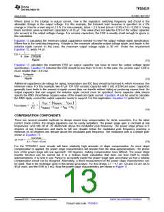
COMPENSATION COMPONENTS
There are several possible methods to design closed loop compensation for dc/dc converters. For the ideal
current mode control, the design equations can be easily simplified. The power stage gain is constant at low
frequencies, and rolls off at -20 dB/decade above the modulator pole frequency. The power stage phase is 0
degrees at low frequencies and starts to fall one decade below the modulator pole frequency reaching a
minimum of -90 degrees one decade above the modulator pole frequency. The modulator pole is a simple pole
shown in Equation 15
Ioutmax
¦p mod =
2p ´ Vout ´ Cout
(15)
For the TPS54531 most circuits will have relatively high amounts of slope compensation. As more slope
compensation is applied, the power stage characteristics will deviate from the ideal approximations. The phase
loss of the power stage will now approach -180 degrees, making compensation more difficult. The power stage
transfer function can be solved but it is a tedious hand calculation that does not lend itself to simple
approximations. It is best to use Pspice to accurately model the power stage gain and phase so that a reliable
compensation circuit can be designed. Alternately, a direct measurement of the power stage characteristics can
be used. That is the technique used in this design procedure. For this design, L1 = 4.7 µH. C8 and C9 are set to
47µF each, and the ESR is 3 mΩ. Now the power stage characteristics are shown in Figure 11.
Copyright © 2013, Texas Instruments Incorporated
Submit Documentation Feedback
13
Product Folder Links: TPS54531

 TI [ TEXAS INSTRUMENTS ]