TPS54531
SLVSBI5 –MAY 2013
www.ti.com
APPLICATION INFORMATION
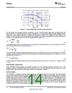
L1 4.7 uH
VOUT 5V, 5A
VOUT
C4
0.1µF
U1
TPS54531
C8
C9
C10
D1
R4
CDBC540-G
47µF
47µF
open
0.55V
51.1
1
8
7
6
5
BOOT
VIN
EN
PH
GND
VIN 8-28VOLTS
2
VIN
R1
3
C1
C2
C3
COMP
665k
4.7µF
4.7µF
0.01µF
C11
C6
R5
4
SS
VSNS
open
2200pF
10.2K
C7
9
PWR PAD
C5
R3
37.4k
R2
22pF
0.01µF
130k
R6
1.96k
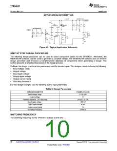
Figure 10. Typical Application Schematic
STEP BY STEP DESIGN PROCEDURE
The following design procedure can be used to select component values for the TPS54531. Alternately, the
WEBENCH® software may be used to generate a complete design. The WEBENCH® software uses an iterative
design procedure and accesses a comprehensive database of components when generating a design. This
section presents a simplified discussion of the design process.
To begin the design process a few parameters must be decided upon. The designer needs to know the following:
•
•
•
•
•
•
Input voltage range
Output voltage
Input ripple voltage
Output ripple voltage
Output current rating
Operating frequency
For this design example, use the following as the input parameters
Table 2. Design Parameters
DESIGN PARAMETER
Input voltage range
EXAMPLE VALUE
8 V to 28V
5 V
Output voltage
Transient response, 2.5 A load step
Input ripple voltage
ΔVout = +/- 5 %
400 mV
Output ripple voltage
Output current rating
Operating Frequency
30 mV
5 A
570 kHz
SWITCHING FREQUENCY
The switching frequency for the TPS54531 is fixed at 570 kHz.
10
Submit Documentation Feedback
Copyright © 2013, Texas Instruments Incorporated
Product Folder Links: TPS54531

 TI [ TEXAS INSTRUMENTS ]