TPS54531
SLVSBI5 –MAY 2013
www.ti.com
RDS(on) is the on-resistance of the high-side MOSFET (Ω).
VOUT is the output voltage (V).
VIN is the input voltage (V).
Fsw is the switching frequency (Hz).
So
Ptot = Pcon + Psw + Pgc + Pq
For given TA , TJ = TA + Rth x Ptot.
For given TJMAX = 150°C, TAMAX = TJMAX– Rth x Ptot.
Where:
Ptot is the total device power dissipation (W).
TA is the ambient temperature (°C).
TJ is the junction temperature (°C) .
Rth is the thermal resistance of the package (°C/W).
TJMAX is maximum junction temperature (°C).
TAMAX is maximum ambient temperature (°C).
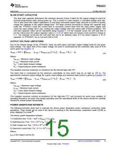
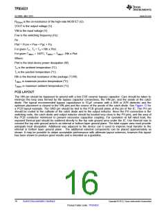
PCB LAYOUT
The VIN pin should be bypassed to ground with a low ESR ceramic bypass capacitor. Care should be taken to
minimize the loop area formed by the bypass capacitor connections, the VIN pin, and the anode of the catch
diode. The typical recommended bypass capacitance is 10-μF ceramic with a X5R or X7R dielectric and the
optimum placement is closest to the VIN pins and the source of the anode of the catch diode. See Figure 12 for
a PCB layout example. The GND pin should be tied to the PCB ground plane at the pin of the IC. The PH pin
should be routed to the cathode of the catch diode and to the output inductor. Since the PH connection is the
switching node, the catch diode and output inductor should be located very close to the PH pins, and the area of
the PCB conductor minimized to prevent excessive capacitive coupling. For operation at full rated load, the
exposed thermal pad should be soldered directly to the top side ground area under the IC. Use thermal vias to
connect the top side ground area to an internal or bottom layer ground plane. The total copper area must provide
adequate heat dissipation. Additional vias adjacent to the device can b used to improve heat transfer to the
infernal or bottom layer ground plane . The additional external components can be placed approximately as
shown. It may be possible to obtain acceptable performance with alternate layout schemes, however this layout
has been shown to produce good results and is intended as a guideline.
16
Submit Documentation Feedback
Copyright © 2013, Texas Instruments Incorporated
Product Folder Links: TPS54531

 TI [ TEXAS INSTRUMENTS ]