TPS54531
www.ti.com
SLVSBI5 –MAY 2013
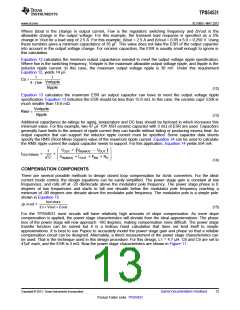
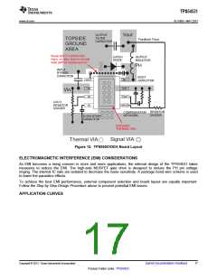
OUTPUT
FILTER
CAPACITOR
Vout
TOPSIDE
GROUND
AREA
Feedback Trace
Route BOOT CAPACITOR
trace on other layer to provide
wide path for topside ground
CATCH
DIODE
OUTPUT
INDUCTOR
PH
INPUT
BYPASS
CAPACITOR
BOOT
CAPACITOR
BOOT
PH
VIN
EN
SS
GND
COMP
Vin
UVLO
RESISTOR
DIVIDER
VSENSE
RESISTOR
DIVIDER
COMPENSATION
NETWORK
SLOW START
CAPACITOR
EXPOSED
THERMAL PAD
Signal VIA
Thermal VIA
Figure 12. TPS54531DDA Board Layout
ELECTROMAGNETIC INTERFERENCE (EMI) CONSIDERATIONS
As EMI becomes a rising concern in more and more applications, the internal design of the TPS54531 takes
measures to reduce the EMI. The high-side MOSFET gate drive is designed to reduce the PH pin voltage
ringing. The internal IC rails are isolated to decrease the noise sensitivity. A package bond wire scheme is used
to lower the parasitics effects.
To achieve the best EMI performance, external component selection and board layout are equally important.
Follow the Step by Step Design Procedure above to prevent potential EMI issues.
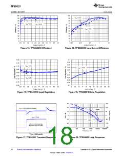
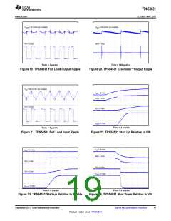
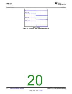
APPLICATION CURVES
spacer
Copyright © 2013, Texas Instruments Incorporated
Submit Documentation Feedback
17
Product Folder Links: TPS54531

 TI [ TEXAS INSTRUMENTS ]