TPS54531
www.ti.com
SLVSBI5 –MAY 2013
SLOPE COMPENSATION
In order to prevent the sub-harmonic oscillations when operating the device at duty cycles greater than 50%, the
TPS54531 adds a built-in slope compensation which is a compensating ramp to the switch current signal.
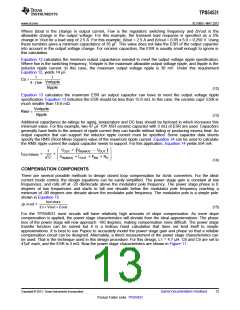
CURRENT MODE COMPENSATION DESIGN
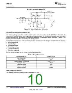
The device is able to work with various types of output capacitors with appropriate compensation designs. For
designs using ceramic output capacitors, proper derating of ceramic output capacitance is recommended when
doing the stability analysis. This is because the actual ceramic capacitance drops considerably from the nominal
value when the applied voltage increases. Please refer to the Step by Step Design Procedure in the Application
Information section for the detailed guidelines.
OVERCURRENT PROTECTION AND FREQUENCY SHIFT
The TPS54531 implements current mode control that uses the COMP pin voltage to turn off the high-side
MOSFET on a cycle by cycle basis. Every cycle the switch current and the COMP pin voltage are compared;
when the peak inductor current intersects the COMP pin voltage, the high-side switch is turned off. During
overcurrent conditions that pull the output voltage low, the error amplifier responds by driving the COMP pin high,
causing the switch current to increase. The COMP pin has a maximum clamp internally, which limit the output
current.
The TPS54531 provides robust protection during short circuits. There is potential for overcurrent runaway in the
output inductor during a short circuit at the output. The TPS54531 solves this issue by increasing the off time
during short circuit conditions by lowering the switching frequency. The switching frequency is divided by 8, 4, 2,
and 1 as the voltage ramps from 0 V to 0.8 V on VSENSE pin. The relationship between the switching frequency
and the VSENSE pin voltage is shown in Table 1.
Table 1. Switching Frequency Conditions
SWITCHING FREQUENCY
570 kHz
VSENSE PIN VOLTAGE
VSENSE ≥ 0.6 V
570 kHz / 2
0.6 V > VSENSE ≥ 0.4 V
0.4 V > VSENSE ≥ 0.2 V
0.2 V > VSENSE
570 kHz / 4
570 kHz / 8
OVERVOLTAGE TRANSIENT PROTECTION
The TPS54531 incorporates an overvoltage transient protection (OVTP) circuit to minimize output voltage
overshoot when recovering from output fault conditions or strong unload transients. The OVTP circuit includes an
overvoltage comparator to compare the VSENSE pin voltage and internal thresholds. When the VSENSE pin
voltage goes above 109% × Vref, the high-side MOSFET will be forced off. When the VSENSE pin voltage falls
below 107% × Vref, the high-side MOSFET will be enabled again.
THERMAL SHUTDOWN
The device implements an internal thermal shutdown to protect itself if the junction temperature exceeds 165°C.
The thermal shutdown forces the device to stop switching when the junction temperature exceeds the thermal
trip threshold. Once the die temperature decreases below 165°C, the device reinitiates the power up sequence.
Copyright © 2013, Texas Instruments Incorporated
Submit Documentation Feedback
9
Product Folder Links: TPS54531

 TI [ TEXAS INSTRUMENTS ]