TPS54531
www.ti.com
SLVSBI5 –MAY 2013
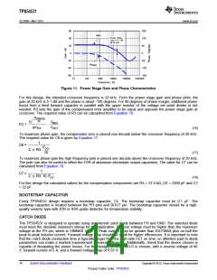
SLOW START CAPACITOR
The slow start capacitor determines the minimum amount of time it takes for the output voltage to reach its
nominal programmed value during power up. This is useful if a load requires a controlled voltage slew rate.
This is also used if the output capacitance is very large and would require large amounts of current to quickly
charge the capacitor to the output voltage level. The large currents necessary to charge the capacitor may
make the TPS54531 reach the current limit or excessive current draw from the input power supply may
cause the input voltage rail to sag. Limiting the output voltage slew rate solves both of these problems. The
soft start capacitor value can be calculated using Equation 3. For the example circuit, the soft start time is
not too critical since the output capacitor value is 2 x 47 μF which does not require much current to charge to
5 V. The example circuit has the soft start time set to an arbitrary value of 4 ms which requires a 10 nF
capacitor. In TPS54531, Iss is 2 µA and Vref is 0.8V.
OUTPUT VOLTAGE LIMITATIONS
Due to the internal design of the TPS54531, there are both upper and lower output voltage limits for any given
input voltage. The upper limit of the output voltage set point is constrained by the maximum duty cycle of 91%
and is given by Equation 19:
VOmax = 0.91 ×
V
- IO max × RDS(on) max + V
)
-
I
(
× RL - VD
)
(
(
)
IN min
D
O max
(19)
Where:
VIN min = Minimum input voltage
IO max = Maximum load current
VD = Catch diode forward voltage
RL = Output inductor series resistance
The equation assumes maximum on resistance for the internal high-side FET.
The lower limit is constrained by the minimum controllable on time which may be as high as 130 ns. The
approximate minimum output voltage for a given input voltage and minimum load current is given by Equation 20:
VOmin = 0.089 ×
V
- IO min × RDS(on) min + V
)
-
I
(
× RL - VD
)
(
(
)
IN max
D
O min
(20)
Where:
VIN max = Maximum input voltage
IO min = Minimum load current
VD = Catch diode forward voltage
RL = Output inductor series resistance
This equation assumes nominal on-resistance for the high-side FET and accounts for worst case variation of
operating frequency set point. Any design operating near the operational limits of the device should be carefully
checked to assure proper functionality.
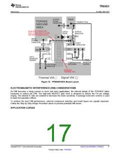
POWER DISSIPATION ESTIMATE
The following formulas show how to estimate the device power dissipation under continuous conduction mode
operations. They should not be used if the device is working in the discontinuous conduction mode (DCM) or
pulse skipping Eco-modeTM
.
The device power dissipation includes:
1) Conduction loss: Pcon = Iout2 x RDS(on) x VOUT/VIN
2) Switching loss: Psw = 0.5 x 10⁻⁹ x VIN 2 x IOUT x Fsw
3) Gate charge loss: Pgc = 22.8 x 10⁻⁹ x Fsw
4) Quiescent current loss: Pq = 0.11 x 10⁻³ x VIN
Where:
IOUT is the output current (A).
Copyright © 2013, Texas Instruments Incorporated
Submit Documentation Feedback
15
Product Folder Links: TPS54531

 TI [ TEXAS INSTRUMENTS ]