TPS54531
SLVSBI5 –MAY 2013
www.ti.com
60
40
20
0
180
120
60
Gain
Power Stage
Gain = 5.1 dB
@ 20 kHz
0
-20
-40
-60
-60
-120
-180
Phase
10
100
1000
10000
100000
1000000
C011
Frequency - Hz
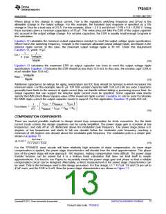
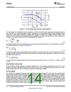
Figure 11. Power Stage Gain and Phase Characteristics
For this design, the intended crossover frequency is 20 kHz. From the power stage gain and phase plots, the
gain at 20 kHz is 5.1 dB and the phase is about -100 degrees. For 60 degrees of phase margin, additional phase
boost from a feed forward capacitor in parallel with the upper resistor of the voltage set point divider is not
needed. R3 sets the gain of the compensated error amplifier to be equal and opposite the power stage gain at
crossover. The required value of R3 can be calculated from Equation 16.
-GPWRSTG
20
VREF
VOUT
10
R3 =
×
gmEA
(16)
To maximize phase gain, the compensator zero is placed one decade below the crossover frequency of 20 kHz.
The required value for C6 is given by Equation 17.
1
C6 =
FCO
2× p×R3×
10
(17)
To maximize phase gain the high frequency pole is placed one decade above the crossover frequency of 20 kHz.
The pole can also be useful to offset the ESR of aluminum electrolytic output capacitors. The value for C7 can be
calculated from Equation 18.
1
C7 =
2× p ×R3×10×FCO
(18)
For this design the calculated values for the compensation components are R3 = 37.4 kΩ ,C6 = 2200 pF and C7
= 22 pF.
BOOTSTRAP CAPACITOR
Every TPS54531 design requires a bootstrap capacitor, C4. The bootstrap capacitor must be 0.1 μF. The
bootstrap capacitor is located between the PH pins and BOOT pin. The bootstrap capacitor should be a high-
quality ceramic type with X7R or X5R grade dielectric for temperature stability.
CATCH DIODE
The TPS54531 is designed to operate using an external catch diode between PH and GND. The selected diode
must meet the absolute maximum ratings for the application: Reverse voltage must be higher than the maximum
voltage at the PH pin, which is VINMAX + 0.5 V. Peak current must be greater than IOUTMAX plus on half the
peak to peak inductor current. Forward voltage drop should be small for higher efficiencies. It is important to note
that the catch diode conduction time is typically longer than the high-side FET on time, so attention paid to diode
parameters can make a marked improvement in overall efficiency. Additionally, check that the device chosen is
capable of dissipating the power losses. For this design, a CDBC540-G is chosen, with a reverse voltage of 40
V, forward current of 5 A, and a forward voltage drop of 0.55 V.
14
Submit Documentation Feedback
Copyright © 2013, Texas Instruments Incorporated
Product Folder Links: TPS54531

 TI [ TEXAS INSTRUMENTS ]