TMS320TCI6487
TMS320TCI6488
Communications Infrastructure Digital Signal Processor
SPRS358F–APRIL 2007–REVISED AUGUST 2008
www.ti.com
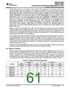
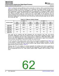
Table 5-2 shows the memory addresses used to access the L2 memory. Cells in normal font should be
used by the software for memory accesses. The L2 addresses are common between all three cores,
allowing for the same code to be run unmodified on each. Cells in italic (N/A) are not accessible. In the
case of asymmetric L2 and C64x+ Megamodule Core 0, the beginning of L2 is mapped to UMAP1 and the
last 0.5MB of L2 to UMAP0. Therefore, the first 32 L2 MPPA registers map to the last part of L2 and vice
versa. Memory protection pages are 1/32nd of the size of each UMAP. For the symmetric case, the
memory protection sizes are constant across all three cores. The asymmetric case, however, has memory
split across multiple ports. Ports that have only 512K will have memory protection pages that are half the
size of ports with 1MB.
Table 5-2. L2 Memory Address Ranges
l2_CONFIG = 0
l2_CONFIG = 1
C64x+
C64x+
C64x+
C64x+
C64x+
C64x+
ADDRESS RANGE
MEGAMODULE MEGAMODULE MEGAMODULE MEGAMODULE MEGAMODULE MEGAMODULE
CORE 0
CORE 1
CORE 2
CORE 0
CORE 1
CORE 2
0x0080 0000 -
0x0087 FFFF
UMAP 1
UMAP 0
UMAP 0
UMAP 0
UMAP 0
UMAP 0
0x0088 0000 -
0x008F FFFF
UMAP 1
UMAP 0
N/A
UMAP 0
N/A
N/A
N/A
N/A
UMAP 0
N/A
UMAP 0
N/A
UMAP 0
N/A
0x0090 0000 -
0x0097 FFFF
0x0098 0000 -
0x009F FFFF
N/A
N/A
N/A
N/A
Each page may be assigned with fully orthogonal user and supervisor read, write, and execute
permissions. Additionally, a page may be marked as either (or both) locally or globally accessible. A local
access is one initiated by the CPU, while a global access is initiated by a DMA (either IDMA or DMA
access by any C64x+ Megamodule or master peripheral). On a secure device, pages can be restricted to
secure accesses only (default) or opened up for public, non-secure access.
The CPU and each of the system masters on the device are all assigned a privilege ID (see Table 5-3). It
is only possible to specify whether the memory pages are locally or globally accessible. The AIDx
(x=0,1,2,3,4,5) and LOCAL bits of the memory protection page attribute registers specify the memory
page protection scheme as listed in Table 5-4.
Whenever the CPU is the initiator of a memory transaction, the privilege mode (user or supervisor) in
which the CPU is running at that time is carried with those transactions. This includes EDMA3 transfers
that are programmed by the CPU. Other system masters (EMAC, RapidIO, RAC) are always in user
mode.
62
C64x+ Megamodule
Submit Documentation Feedback

 TI [ TEXAS INSTRUMENTS ]