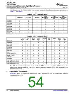
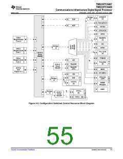
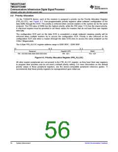
TMS320TCI6487
TMS320TCI6488
Communications Infrastructure Digital Signal Processor
SPRS358F–APRIL 2007–REVISED AUGUST 2008
www.ti.com
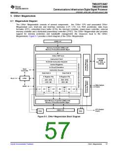
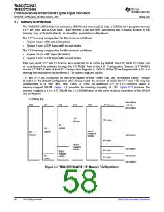
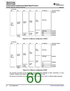
5.2 Memory Architecture
The TMS320TCI6487/8 device contains a 3MB level-2 memory (L2) total, a 32KB level-1 program memory
(L1P) per core, and a 32KB level-1 data memory (L1D) per core. All memory has a unique location in the
memory map and can be directly accessed by any master on the device.
The L1P memory configuration for the device is as follows:
•
•
Region 0 size is 0K bytes (disabled).
Region 1 size is 32K bytes with no wait states.
The L1D memory configuration for the device is as follows:
•
•
Region 0 size is 0K bytes (disabled).
Region 1 size is 32K bytes with no wait states.
After core reset, L1P and L1D cache are configured as all cache by default. The L1P and L1D cache can
be reconfigured via software through the L1PMODE field of the L1P Configuration Register (L1PMODE)
and the L1DMODE field of the L1D Configuration Register (L1DCFG) of the C64x+ Megamodule. L1D is a
two-way set-associative cache while L1P is a direct-mapped cache.
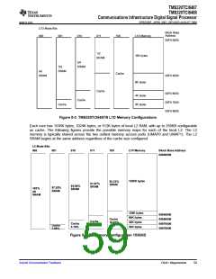
L1P and L1D are configured as memory-mapped SRAM, rather than only unmapped cache. Though
all-cache is the default configuration after device reset, the amount of cache for L1P and L1D may be
programmed to be 0Kb, 4Kb, 8Kb, 16Kb, or 32Kb. All additional L1P or L1D memory space is
memory-mapped SRAM. Figure 5-2 provides the memory mapping of L1P. Figure 5-2 provides the
memory mapping of L1D. L1P SRAM and L1D SRAM begin at the same address regardless of the SRAM
size configured.
L1P Mode Bits
Block Base
Address
000
001
010
011
100
L1P Memory
00E0 0000
1/2
16K bytes
SRAM
3/4
SRAM
7/8
direct
mapped
cache
SRAM
All
SRAM
00E0 4000
8K bytes
direct
mapped
cache
00E0 6000
00E0 7000
00E0 8000
4K bytes
4K bytes
direct
mapped
cache
dm
cache
Figure 5-2. TMS320TCI6487/8 L1P Memory Configurations
58
C64x+ Megamodule
Submit Documentation Feedback

 TI [ TEXAS INSTRUMENTS ]