TMS320TCI6487
TMS320TCI6488
Communications Infrastructure Digital Signal Processor
SPRS358F–APRIL 2007–REVISED AUGUST 2008
www.ti.com
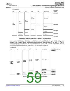
L2 Mode Bits
000
001
010
011
100
L1P Memory
Block Base Address
00800000
768K bytes
75%
SRAM
87.5%
SRAM
93.75%
SRAM
96.875%
SRAM
100%
All
SRAM
128K bytes
64K
008C0000
008E0000
008F0000
008F8000
Cache
25%
Cache
12.5%
32 K
Cache
6.25%
Cache
32 K
3.125%
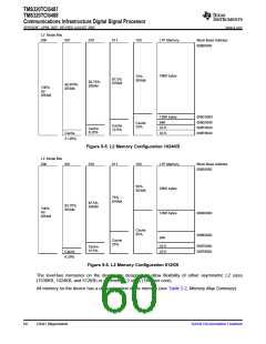
Figure 5-5. L2 Memory Configuration 1024KB
L2 Mode Bits
000
001
010
011
100
L1P Memory
256K bytes
128K bytes
64K
Block Base Address
00800000
50%
SRAM
75%
SRAM
87.5%
SRAM
93.75%
SRAM
100%
All
SRAM
00840000
00860000
Cache
50%
Cache
25%
32 K
32 K
00870000
00878000
Cache
12.5%
Cache
6.25%
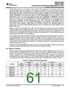
Figure 5-6. L2 Memory Configuration 512KB
The level-two memories on the device are designed to allow flexibility of either asymmetric L2 sizes
(1536KB, 1024KB, and 512KB) or symmetric L2 sizes (1MB per core).
All memory on the device has a unique location in the memory (see Table 2-2, Memory Map Summary).
60
C64x+ Megamodule
Submit Documentation Feedback

 TI [ TEXAS INSTRUMENTS ]