TMS320TCI6487
TMS320TCI6488
Communications Infrastructure Digital Signal Processor
www.ti.com
SPRS358F–APRIL 2007–REVISED AUGUST 2008
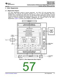
Global addresses that are accessible to all masters in the system are in all memory local to the
processors. Additionally, local memory can be accessed directly by the associated processor through
aliased addresses, where the eight MSBs are masked to zero. The aliasing is handled within the C64x+
Megamodule and allows for common code to be run unmodified on multiple cores. For example, address
location 0x10800000 is the global base address for C64x+ Megamodule Core 0's L2 memory. C64x+
Megamodule Core 0 can access this location by either using 0x10800000 or 0x00800000. Any other
master on the device must use 0x10800000 only. Conversely, 0x00800000 can by used by any of the
three cores as their own L2 base addresses. For C64x+ Megamodule Core 0, as mentioned this is
equivalent to 0x10800000, for C64x+ Megamodule Core 1 this is equivalent to 0x11800000, and for
C64x+ Megamodule Core 2 this is equivalent to 0x12800000. Local addresses should only be used for
shared code or data, allowing a single image to be included in memory. Any code/data targeted to a
specific core, or a memory region allocated during run-time by a particular core should always use the
global address only.
When accessing the internal ROM of the DSP, the CPU frequency must always be less than 750 MHz.
Therefore, when using a software boot mode, care must be taken so that the CPU frequency does not
exceed 750 MHz at any point during the boot sequence. After the boot sequence has completed, the CPU
frequency can be programmed to the frequency required by the application. For more detailed information
on boot modes, see Section 2.4, Boot Sequence.
The L3 ROM on the device is 64KB. The contents of the ROM are divided into two partitions. The first is
the ROM bootloader with the primary purpose to contain software to boot the device. There is no
requirement to block accesses from this portion to the ROM. The second partition is the secure portion of
ROM which has a secure kernel which is necessary for support of security features on the device. For the
secure portion, access should not be allowed on a non-secure part and on a secure part, only secure
supervisors should have access.
Emulation accesses should follow the same rules of the secure portion of ROM. Emulation can access the
non-secure portion of the ROM, but can not read the secure portion of the ROM.
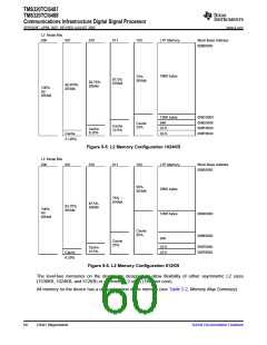
5.3 Memory Protection
Memory protection allows an operating system to define who or what is authorized to access L1D, L1P,
and L2 memory. To accomplish this, the L1D, L1P, and L2 memories are divided into pages. There are 16
pages of L1P (2KB each), 16 pages of L1D (2KB each), and up to 64 pages of L2. The L1D, L1P, and L2
memory controllers in the C64x+ Megamodule are equipped with a set of registers that specify the
permissions for each memory page. For L2, the number of protection pages and their sizes depend on the
L2 configuration of the device, as defined in the previous section. The actual sizes are listed in Table 5-1.
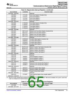
Table 5-1. L2 Memory Protection Page Sizes
L2CONFIG = 0
L2CONFIG = 1
C64x+
C64x+
C64x+
C64x+
C64x+
C64x+
ADDRESS
MEGAMODULE MEGAMODULE MEGAMODULE MEGAMODULE MEGAMODULE MEGAMODULE
CORE 0
CORE 1
CORE 2
CORE 0
CORE 1
CORE 2
0x0080 0000 -
0x0087 FFFF
32 KB
32 KB
16 KB
32 KB
32 KB
32 KB
0x0088 0000 -
0x008F FFFF
32 KB
16 KB
N/A
32 KB
N/A
N/A
N/A
N/A
32 KB
N/A
32 KB
N/A
32 KB
N/A
0x0090 0000 -
0x0097 FFFF
0x0098 0000 -
0x009F FFFF
N/A
N/A
N/A`
N/A
Submit Documentation Feedback
C64x+ Megamodule
61

 TI [ TEXAS INSTRUMENTS ]