TMS320TCI6487
TMS320TCI6488
Communications Infrastructure Digital Signal Processor
www.ti.com
SPRS358F–APRIL 2007–REVISED AUGUST 2008
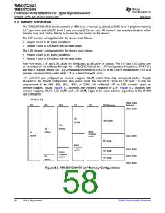
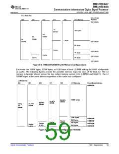
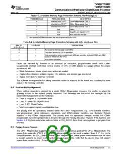
L1D Mode Bits
000
Block Base
Address
001
010
011
100
L1D Memory
00F0 0000
1/2
16K bytes
SRAM
3/4
SRAM
7/8
SRAM
All
Cache
SRAM
00F0 4000
8K bytes
Cache
00F0 6000
00F0 7000
00F0 8000
4K bytes
4K bytes
Cache
Cache
Figure 5-3. TMS320TCI6487/8 L1D Memory Configurations
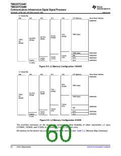
Each core has 1536K bytes, 1024K bytes, or 512K bytes of local L2 RAM, with up to 256KB configurable
as cache. The following figures provide the possible memory maps for each of the local L2. The L2
memory is typically shared across the two unified memory access ports (UMAP0 and UMAP1). The L2
SRAM begins at the same address regardless of the cache size configured.
L2 Mode Bits
000
001
010
011
100
L1P Memory
Block Base Address
00800000
1280K bytes
83.33%
SRAM
91.67%
SRAM
95.84%
SRAM
97.92%
SRAM
100%
All
SRAM
128K bytes
64K bytes
32K bytes
32K bytes
00940000
00960000
00970000
00978000
Cache
Cache
8.33%
16.67%
Cache
4.16%
Cache
2.08%
Figure 5-4. L2 Memory Configuration 1536KB
Submit Documentation Feedback
C64x+ Megamodule
59

 TI [ TEXAS INSTRUMENTS ]