TMS320TCI6487
TMS320TCI6488
Communications Infrastructure Digital Signal Processor
SPRS358F–APRIL 2007–REVISED AUGUST 2008
www.ti.com
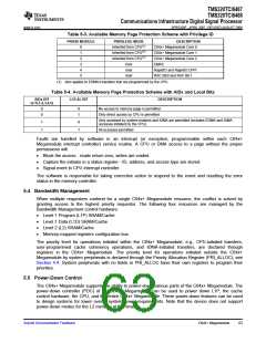
5.6 Megamodule Resets
Table 5-5 shows the reset types supported on the device and if the resetting affects the Megamodule
globally or just locally.
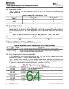
Table 5-5. Megamodule Reset (Global or Local)
RESET TYPE
Power-On
Warm
GLOBAL RESET
LOCAL RESET
Y
Y
Y
N
Y
Y
Y
Y
System
CPU
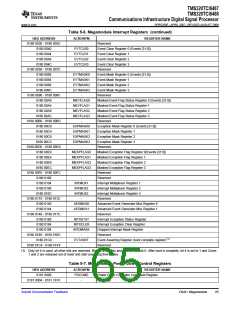
5.7 Megamodule Revision
The version and revision of the C64x+ Megamodule can be read from the Megamodule Revision ID
Register (MM_REVID) located at address 0181 2000h. The MM_REVID register is shown in Figure 5-7
and described in Section 5.8. The C64x+ Megamodule revision is dependant on the silicon revision being
used.
Figure 5-7. Megamodule Revision ID Register (MM_REVID) [Hex Address: 0181 2000h]
31
16 15
0
VERSION
R-3h
REVISION(1)
R-n
LEGEND: R/W = Read/Write; R = Read only; -n = value after reset
(1) The C64x+ Megamodule revision is dependent on the silicon revision being used.
Table 5.8. Megamodule Revision ID Register (MM_REVID) Field Descriptions
BIT
31:16
15:0
FIELD
VALUE
DESCRIPTION
VERSION
REVISION
3H
Version of the C64x+ Megamodule implemented on the device. This field is always read as 3h.
Revision of the C64x+ Megamodule version implemented on the device. The C64x+ Megamodule
revision is dependent on the silicon revision being used.
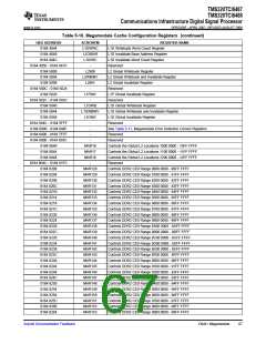
5.9 C64X+ Megamodule Register Description(s)
In some applications, some specific addresses may need to be read from their physical locations each
time they are accessed (e.g., a status register within FPGA).
The L2 controller offers registers that control whether certain ranges of memory are cacheable and
whether one or more requestors are actually permitted to access these ranges. The registers are referred
to as memory attribute registers (MARs). A list of MARs is provided in Table 5-10.
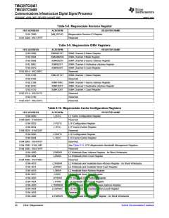
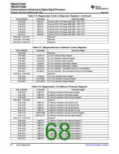
Table 5-6. Megamodule Interrupt Registers
HEX ADDRESS
0180 0000
ACRONYM
EVTFLAG0
EVTFLAG1
EVTFLAG2
EVTFLAG3
-
REGISTER NAME
Event Flag Register 0 (Events [31:0])
0180 0004
Event Flag Register 1
Event Flag Register 2
Event Flag Register 3
Reserved
0180 0008
0180 000C
0180 0010 - 0180 001C
0180 0020
EVTSET0
EVTSET1
EVTSET2
EVTSET3
Event Set Register 0 (Events [31:0])
Event Set Register 1
Event Set Register 2
Event Set Register 3
0180 0024
0180 0028
0180 002C
64
C64x+ Megamodule
Submit Documentation Feedback

 TI [ TEXAS INSTRUMENTS ]