TMS320TCI6487
TMS320TCI6488
Communications Infrastructure Digital Signal Processor
SPRS358F–APRIL 2007–REVISED AUGUST 2008
www.ti.com
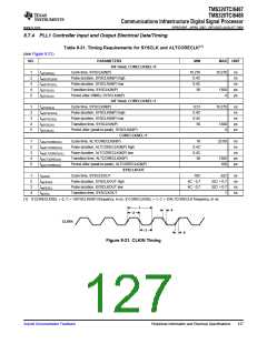
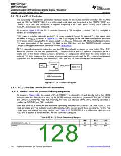
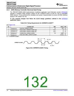
8.8 PLL2 and PLL2 Controller
The secondary PLL controller generates interface clocks for the DDR2 memory controller. The CLKIN2
input for PLL2 is DDRREFCLK. It is a differential clock input and is applied at the DDRREFCLKP and
DDRREFCLKN pins. The DDRREFCLK required frequency is 66.7 MHz. When coming out of power-on
reset, PLL2 is enabled and initialized.
As shown in Figure 8-22, the PLL2 controller features a PLL multiplier controller. The PLL multiplier is
fixed to a x10 multiplier rate.
PLL2 power is supplied externally via the PLL2 power supply (AVDD218). An external PLL filter circuit must
be added to AVDD218 as shown in Figure 8-22. The 1.8-V supply for the EMI filter must be from the same
1.8-V power plane supplying the I/O power-supply pin, DVDD18. TI requires EMI filter manufacturer Murata.
For more information on the external PLL filter or the EMI filter, see the TMS320TCI6488 Hardware
Design Guide application report (literature number SPRAAG5).
All PLL external components (capacitors and the EMI filter) should be placed as close to the C64x+ DSP
device as possible. For the best performance, TI requires that all the PLL external components be on a
single side of the board without jumpers, switches, or components other than the ones shown. For
reduced PLL jitter, maximize the spacing between switching signals and the PLL external components
(capacitors and the EMI filter). The minimum CLKIN2 rise and fall times should also be observed.
DDR.PLL
AVDD218
DDR_2XCLK
DDR2 PHY
x10
DDR.PLLController
Figure 8-22. PLL2 Block Diagram
8.8.1 PLL2 Controller Device-Specific Information
8.8.1.1 Internal Clocks and Maximum Operating Frequencies
As shown in Figure 8-22, the output of PLL2, PLLOUT, is divided by 2 and directly fed to the DDR2
memory controller. This clock is used by the DDR2 memory controller to generate DDR2CLKOUT0[P/N]
and DDR2CLKOUT1[P/N]. Note that, internally, the data bus interface of the DDR2 memory controller is
clocked by SYSCLK2 and PLL1 controller.
Note that there is a minimum and maximum operating frequency for DDRREFCLK and PLLOUT. The
clock generator and PLL multiplier must not be configured to exceed any of these constraints. For the PLL
clocks input and output frequency ranges, see Table 8-32. DDRREFCLK is a differential clock input to
PLL2 and is applied at the DDRREFCLKP and DDRREFCLKN pins.
Table 8-32. PLL2 Clock Frequency Ranges
MIN
40
MAX
66.7
667
UNIT
Mz
DDRREFCLK (PLLEN = 1)
PLLOUT
400
MHz
128
Peripheral Information and Electrical Specifications
Submit Documentation Feedback

 TI [ TEXAS INSTRUMENTS ]