TMS320TCI6487
TMS320TCI6488
Communications Infrastructure Digital Signal Processor
SPRS358F–APRIL 2007–REVISED AUGUST 2008
www.ti.com
8.9 DDR2 Memory Controller
The 32-bit DDR2 Memory Controller bus of the TCI6487/8 device is used to interface to JESD79-2B
standard-compliant DDR2 SDRAM devices. The DDR2 bus is designed to sustain a throughput of up to
2.67 GBps at a 667-MHz data rate (333-MHz clock rate) as long as data requests are pending in the
DDR2 Memory Controller.
The DDR2 external bus only interfaces to DDR2 SDRAM devices; it does not share the bus with any other
types of peripherals.
8.9.1 DDR2 Memory Controller Device-Specific Information
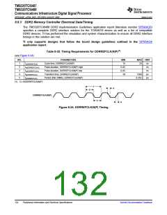
The approach to specifying interface timing for the DDR2 memory bus is different than on other interfaces
such as McBSP. For these other interfaces the device timing was specified in terms of data manual
specifications and I/O buffer information specification (IBIS) models.
For the TCI6487/8 DDR2 memory bus, the approach is to specify compatible DDR2 devices and provide
the printed circuit board (PCB) solution and guidelines directly to the user. Texas Instruments (TI) has
performed the simulation and system characterization to ensure all DDR2 interface timings in this solution
are met. The complete DDR2 system solution is documented in the TMS320TCI6488 DDR2
Implementation Guidelines application report (literature number SPRAAG6).
TI only supports designs that follow the board design guidelines outlined in the SPRAAG6
application report.
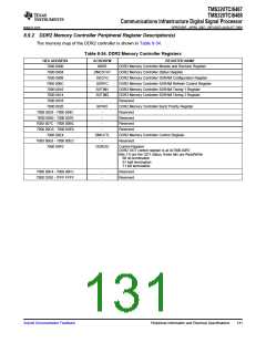
The DDR2 memory controller on the TCI6487/8 device supports the following memory topologies:
•
•
32-bit wide configuration interfacing to two 16-bit wide DDR2 SDRAM devices.
16-bit wide configuration interfacing to a single 16-bit wide DDR2 SDRAM device.
A race condition may exist when certain masters write data to the DDR2 memory controller. For example,
if master A passes a software message via a buffer in external memory and does not wait for indication
that the write completes, when master B attempts to read the software message, then the master B read
may bypass the master A write and, thus, master B may read stale data and, therefore, receive an
incorrect message.
Some master peripherals (e.g., EDMA3 transfer controllers) will always wait for the write to complete
before signaling an interrupt to the system, thus avoiding this race condition. For masters that do not have
hardware specification of write-read ordering, it may be necessary to specify data ordering via software.
If master A does not wait for an indication that a write is complete, it must perform the following
workaround:
1. Perform the required write.
2. Perform a dummy write to the DDR2 memory controller module ID and revision register.
3. Perform a dummy read to the DDR2 memory controller module ID and revision register.
4. Indicate to master B that the data is ready to be read after completion of the read in step 3. The
completion of the read in step 3 ensures that the previous write was done.
130
Peripheral Information and Electrical Specifications
Submit Documentation Feedback

 TI [ TEXAS INSTRUMENTS ]