TMS320TCI6487
TMS320TCI6488
Communications Infrastructure Digital Signal Processor
SPRS358F–APRIL 2007–REVISED AUGUST 2008
www.ti.com
8.9.3 DDR2 Memory Controller Electrical Data/Timing
The TMS320TCI6488 DDR2 Implementation Guidelines application report (literature number SPRAAG6)
specifies a complete DDR2 interface solution for the TCI6487/8 device as well as a list of compatible
DDR2 devices. TI has performed the simulation and system characterization to ensure all DDR2 interface
timings in this solution are met.
TI only supports designs that follow the board design guidelines outlined in the SPRAAG6
application report.
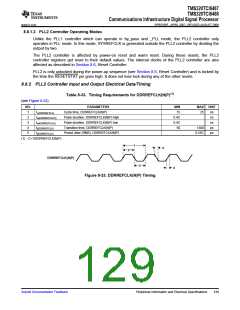
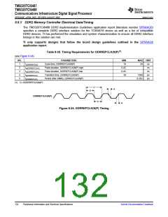
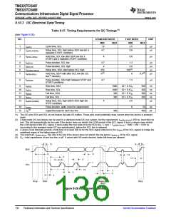
Table 8-35. Timing Requirements for DDRREFCLK(N|P)(1)
(see Figure 8-24)
NO.
1
PARAMETERS
MIN
15
MAX UNIT
tc(DDRREFCLK)
tw(DDRREFCLKH)
tw(DDRREFCLKL)
tt(DDRREFCLK)
tj(DDRREFCLK)
Cycle time, DDRREFCLK(N|P)
25
ns
ns
ns
ps
ps
2
Pulse duration, DDRREFCLK(N|P) high
Pulse duration, DDRREFCLK(N|P) low
Transition time, DDRREFCLK(N|P)
Period Jitter (RMS), DDRREFCLK(N|P)
0.4C
0.4C
50
3
4
1300
5
0.25C
(1) C=1/DDRREFCLK(N|P)
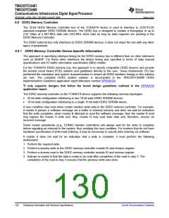
1
4
2
DDRREFCLK(N|P)
3
4
Figure 8-24. DDRREFCLK(N|P) Timing
132
Peripheral Information and Electrical Specifications
Submit Documentation Feedback

 TI [ TEXAS INSTRUMENTS ]