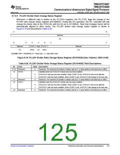
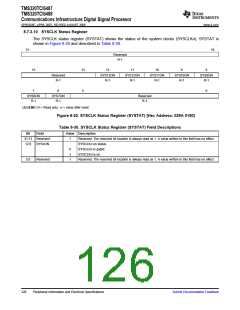
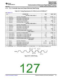
TMS320TCI6487
TMS320TCI6488
Communications Infrastructure Digital Signal Processor
www.ti.com
SPRS358F–APRIL 2007–REVISED AUGUST 2008
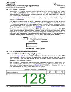
8.8.1.2 PLL2 Controller Operating Modes
Unlike the PLL1 controller which can operate in by_pass and _PLL mode, the PLL2 controller only
operates in PLL mode. In this mode, SYSREFCLK is generated outside the PLL2 controller by dividing the
output by two.
The PLL2 controller is affected by power-on reset and warm reset. During these resets, the PLL2
controller registers get reset to their default values. The internal clocks of the PLL2 controller are also
affected as described in Section 8.6, Reset Controller.
PLL2 is only unlocked during the power-up sequence (see Section 8.6, Reset Controller) and is locked by
the time the RESETSTAT pin goes high. It does not lose lock during any of the other resets.
8.8.2 PLL2 Controller Input and Output Electrical Data/Timing
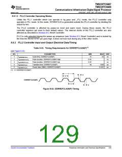
Table 8-33. Timing Requirements for DDRREFCLK(N|P)(1)
(see Figure 8-23)
NO.
1
PARAMETERS
MIN
15
MAX UNIT
tc(DDRREFCLK)
tw(DDRREFCLKH)
tw(DDRREFCLKL)
tt(DDRREFCLK)
tj(DDRREFCLK)
Cycle time, DDRREFCLK(N|P)
25
ns
ns
ns
ps
ps
2
Pulse duration, DDRREFCLK(N|P) high
Pulse duration, DDRREFCLK(N|P) low
Transition time, DDRREFCLK(N|P)
Period Jitter (RMS), DDRREFCLK(N|P)
0.4C
0.4C
50
3
4
1300
5
0.25C
(1) C=1/DDRREFCLK(N|P)
1
4
2
DDRREFCLK(N|P)
3
4
Figure 8-23. DDRREFCLK(N|P) Timing
Submit Documentation Feedback
Peripheral Information and Electrical Specifications
129

 TI [ TEXAS INSTRUMENTS ]