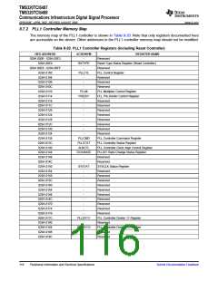
TMS320TCI6487
TMS320TCI6488
Communications Infrastructure Digital Signal Processor
SPRS358F–APRIL 2007–REVISED AUGUST 2008
www.ti.com
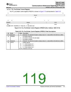
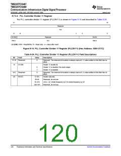
8.7.3.4 PLL Controller Divider 11 Register
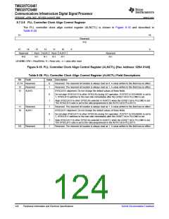
The PLL controller divider 11 register (PLLDIV11) is shown in Figure 8-14 and described in Table 8-24.
31
16
Reserved
R-0
15
14
5
4
0
D11EN
R/W-1
Reserved
R-0
RATIO
R/W-3
LEGEND: R/W = Read/Write; R = Read only; -n = value after reset
Figure 8-14. PLL Controller Divider 11 Register (PLLDIV11) [Hex Address: 029A 017C]
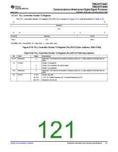
Table 8-24. PLL Controller Divider 11 Register (PLLDIV11) Field Descriptions
Bit
Field
Value
Description
31:16 Reserved
0
Reserved. The reserved bit location is always read as 0. A value written to this field has no
effect.
15
D11EN
Divider 11 enable bit.
0
1
0
Divider 11 is disabled. No clock output.
Divider 11 is enabled.
14:5
4:0
Reserved
RATIO
Reserved. The reserved bit location is always read as 0. A value written to this field has no
effect.
0-1Fh
0h-4h
Divider ratio bits.
Reserved, do not use.
5h-31h
32h-1Fh
÷6 to ÷ 32. Divide frequency by 6 to divide frequency by 32.
Reserved, do not use.
120
Peripheral Information and Electrical Specifications
Submit Documentation Feedback

 TI [ TEXAS INSTRUMENTS ]