TMS320DM6437
Digital Media Processor
www.ti.com
SPRS345B–NOVEMBER 2006–REVISED MARCH 2007
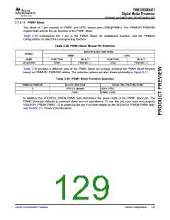
3.7.3.11 PWM1 Block
This block of 1 pin consists of PWM1 and GPIO muxed pins (GP[4]/PWM1). The PINMUX1.PWM1BK
register field selects the pin function in the PWM1 Block.
Table 3-38 summarizes the 1 pin in the PWM1 Block, its multiplexed function, and the PINMUX
configurations to select the corresponding function.
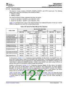
Table 3-38. PWM1 Block Muxed Pin Selection
MULTIPLEXED FUNCTIONS
SIGNAL
PWM1
GPIO
NAME
FUNCTION
SELECT
FUNCTION
SELECT
GP[4]/PWM1
PWM1
PWM1BK = 1
GP[4]
PWM1BK = 0
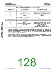
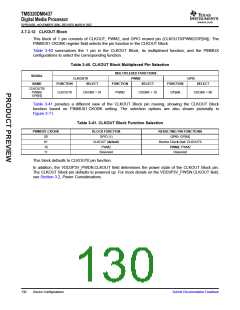
Table 3-39 provides a different view of the PWM1 Block pin muxing, showing the PWM1 Block function
based on PINMUX1.PWM1BK setting. The selection options are also shown pictorially in Figure 3-11.
Table 3-39. PWM1 Block Function Selection
PINMUX1.PWM1BK
BLOCK FUNCTION
GPIO (1) (default)
PWM1
RESULTING PIN FUNCTIONS
GPIO: GP[4]
PWM1: PWM1
0
1
In addition, the VDD3P3V_PWDN.PWM1 field determines the power state of the PWM1 Block pin. The
PWM1 Block pin defaults to powered down and not operational. To use this pin, user must first program
VDD3P3V_PWDN.PWM1 = 0 to power up the pin. For more details on the VDD3P3V_PWDN.PWM1 field,
see Section 3.2, Power Considerations.
Submit Documentation Feedback
Device Configurations
129

 TI [ TEXAS INSTRUMENTS ]