TMS320DM6437
Digital Media Processor
www.ti.com
SPRS345B–NOVEMBER 2006–REVISED MARCH 2007
3.7.3.13 EMIFA/VPSS Block Muxing
This block of 61 pins consists of VPSS, EMIFA, PCI, and GPIO muxed pins. The following register fields
affect the pin functions in the EMIFA/VPSS Block:
•
All PINMUX0 register fields: AEM, VENCSEL, CS5SEL, CS4SEL, CS3SEL, RGBSEL, VPBECKEN,
AEAW, CCDCSEL, HVDSEL, CWENSEL, CFLDSEL, CI76SEL, CI54SEL, CI32SEL, CI10SEL
•
PINMUX1.PCIEN
The EMIFA/VPSS Block is divided into multiple sub-blocks for ultimate flexibility in pin multiplexing to
accommodate a wide variety of applications:
•
•
•
•
Sub-Block 0: multiplexed between VPFE, EMIFA data/address/control pins, PCI, and GPIO.
Sub-Block 1: multiplexed between VPBE, EMIFA data/address/control pins, and GPIO.
Sub-Block 2: no multiplexing. EMIFA control pins EM_WAIT/(RDY/BSY), EM_OE, EM_WE.
Sub-Block 3: multiplexed between EMIFA address pins EM_A[12:6], PCI, and GPIO.
As discussed in Section 3.7.3.2, Peripherals Spanning Multiple Pin Mux Blocks, PCI pins span across the
following Pin Mux Blocks: Host Block, EMIFA/VPSS Block Sub-Block 0 and Sub-Block 3, PCI Data Block,
and GPIO Block. For proper PCI operation, PCI must be selected in all of these Pin Mux Blocks.
The EMBK0, EMBK1, EMBK2, EMBK3 fields in the VDD3P3V_PWDN register determine the power state
of the EMIFA/VPSS Block pins. The EMIFA/VPSS Block pins default to powered up. For more details on
the EMBK0, EMBK1, EMBK2, EMBK3 fields in the VDD3P3V_PWDN register, see Section 3.2, Power
Considerations.
To understand pin multiplexing in the EMIFA/VPSS Block, the user should start with Section 3.7.3.13.1,
EMIFA/VPSS Block Pin Selection Procedure, which outlines the procedures to select pin functions of this
block. Section 3.7.3.13.7, EMIFA/VPSS Block Pin-By-Pin Multiplexing Summary, provides a pin-by-pin
multiplexing summary for the EMIFA/VPSS Block. For more information on the PINMUX0 and PINMUX1
registers, see Section 3.7.2, Pin Muxing Selection After Device Reset.
3.7.3.13.1 EMIFA/VPSS Block Pin Selection Procedure
Follow the steps below to perform pin selection for the EMIFA/VPSS Block and its sub-blocks.
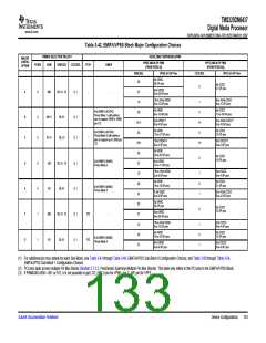
1. Major Configuration Options: start with Table 3-42, EMIFA/VPSS Block Major Configuration Choices.
Based on the peripheral needs, the user should select from the major configuration options in this
block: Major Config Options A, B, C, D, E, F, G.
2. Sub-Block 2 and Sub-Block 3 Selection: After selecting the major configuration option from
Table 3-42, EMIFA/VPSS Block Major Configuration Choices, the pin selection for Sub-Block 2 and
Sub-Block 3 is complete.
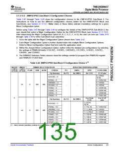
3. Sub-Block 0 Selection: Use Table 3-43 through Table 3-49, EMIFA/VPSS Sub-Block 0 Configuration
Choices, to refine Sub-Block 0 pin selections.
a. Go to the table with the Major Configuration Option chosen in Step 1.
b. Each Major Configuration Option is further divided down into multiple Minor Configuration Options.
Select a Minor Configuration Option that best suits the application need.
c. Within the chosen Minor Configuration Option, further refine the detailed pin configurations by
selecting the settings of PINMUX0 fields CCDCSEL, HVDSEL, CWENSEL, CFLDSEL, CI10SEL,
CI32SEL, CI54SEL, and CI76SEL.
d. The Selection Fields columns show the settings needed to program the PINMUX0 register and
PINMUX1.PCIEN field.
4. Sub-Block 1 Selection: Use Table 3-50 through Table 3-54, EMIFA/VPSS Sub-Block 1 Configuration
Choices, to refine Sub-Block 1 pin selection.
a. Go to the table with the Major Configuration Option chosen in Step 1.
b. Each Major Configuration Option is further divided down into multiple Minor Configuration Options.
Select a Minor Configuration Option that best suits the application need.
c. Within the chosen Minor Configuration Option, further refine the detailed pin configurations by
Submit Documentation Feedback
Device Configurations
131

 TI [ TEXAS INSTRUMENTS ]