TMS320DM6437
Digital Media Processor
www.ti.com
SPRS345B–NOVEMBER 2006–REVISED MARCH 2007
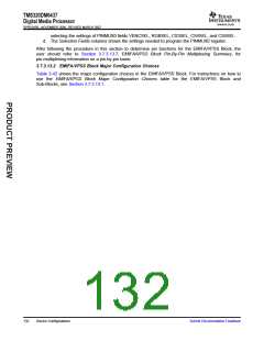
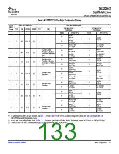
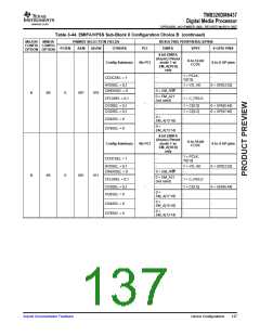
Table 3-42. EMIFA/VPSS Block Major Configuration Choices
PINMUX SELECTION FIELDS(1)
RESULTING PERIPHERALS/PINS
VPBE AND # GP PINS
MAJOR
CONFIG.
OPTION
VPFE AND # GP PINS
(FROM GP[54:34])
PCIEN
AEM
VENCSEL
CCDCSEL
PCI(2)
EMIFA
(FROM GP[33:5])
VENCSEL
VPBE & # GP Pins
CCDCSEL
VPFE & # GP Pins
No VENC
29 GP pins
00
No CCDC
21 GP pins
0
8-bit VENC
8-to-29-GP pins
A
0
000
00, 01, 10
0, 1
-
-
01
10
16-to-24-bit VENC
0-to-12 GP pins
8-to-16-bit CCDC
0-to-12 GP pins
1
0
No VENC
9-to-13 GP pins
No CCDC
11-to-19 GP pins
8-bit EMIFA (ASYNC)
Pinout Mode 1 with address
pins to support 32KB to 16MB
per CS.
00
B
C
0
0
001(3)
00, 01
00, 10
0, 1
0, 1
-
-
8-bit VENC(3)
0-to-4 GP pins
8-to-16-bit CCDC(3)
0-to-10 GP pins
01(3)
00
1(3)
0
No VENC
17-to-21 GP pins
No CCDC
12 GP pins
8-bit EMIFA (ASYNC)
Pinout Mode 3 with address
pins to support up to 32KB per
CS.
011(3)
16-bit VENC(3)
0-to-4 GP pins
8-bit CCDC(3)
0-to-3 GP pins
10(3)
00
1(3)
No VENC
22-to-26 GP pins
No CCDC
13 GP pins
0
8-bit EMIFA (NAND)
Pinout Mode 4
8-bit VENC
12-to-17 GP pins
D
E
F
0
0
1
1
100
101
000
101
00, 01, 10
0, 1
0, 1
0, 1
0, 1
-
01
16-to-18-bit VENC
2-to-9 GP pins
8-bit CCDC
0-to-4 GP pins
10
1
0
1
No VENC
14-to-18 GP pins
No CCDC
21 GP pins
00
8-bit EMIFA (NAND)
Pinout Mode 5
00, 01
-
8- bit VENC
4-to-9 GP pins
8-to-16-bit CCDC
0-to-12 GP pins
01
No VENC
29 GP pins
00
No CCDC
13 GP pins
0
8-bit VENC
8-to-29 GP pins
00, 01, 10
PCI
PCI
-
01
16-to-24-bit VENC
0-to-12 GP pins
8-bit CCDC
0-to-4 GP pins
10
1
0
1
No VENC
14-to-18 GP pins
No CCDC
13 GP pins
00
8-bit EMIFA (NAND)
Pinout Mode 5
G
00, 01
8-bit VENC
4-to-9 GP pins
8-bit CCDC
0-to-4 GP pins
01
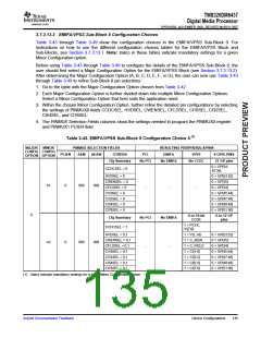
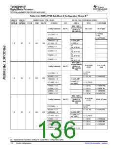
(1) For additional pin mux details for each Sub-Block, see Table 3-43 through Table 3-49, EMIFA/VPSS Sub-Block 0 Configuration Choices, and Table 3-50 through Table 3-54,
EMIFA/VPSS Sub-Block 1 Configuration Choices.
(2) PCI pins span across multiple Pin Mux Blocks (Section 3.7.3.2, Peripherals Spanning Multiple Pin Mux Blocks). This table only refers to the PCI pins in the EMIFA/VPSS Block.
(3) If PINMUX0.AEM = 001 or 011, it is not possible to get LCD_FIELD pin for VPBE, nor C_WE pin for VPFE.
Submit Documentation Feedback
Device Configurations
133

 TI [ TEXAS INSTRUMENTS ]