TMS320DM6437
Digital Media Processor
www.ti.com
SPRS345B–NOVEMBER 2006–REVISED MARCH 2007
3.7.3.12 CLKOUT Block
This block of 1 pin consists of CLKOUT, PWM2, and GPIO muxed pin (CLKOUT0/PWM2/GP[84]). The
PINMUX1.CKOBK register field selects the pin function in the CLKOUT Block.
Table 3-40 summarizes the 1 pin in the CLKOUT Block, its multiplexed function, and the PINMUX
configurations to select the corresponding function.
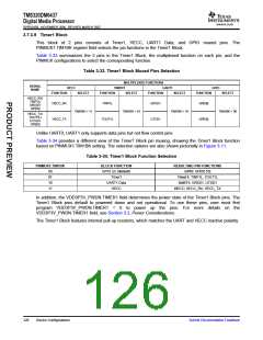
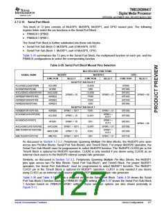
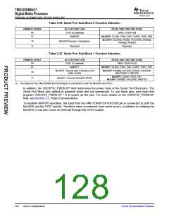
Table 3-40. CLKOUT Block Multiplexed Pin Selection
MULTIPLEXED FUNCTIONS
SIGNAL
CLKOUT0
SELECT
PWM2
GPIO
NAME
FUNCTION
FUNCTION
SELECT
CKOBK = 10
FUNCTION
SELECT
CLKOUT0/
PWM2/
CLKOUT0
CKOBK = 01
PWM2
GP[84]
CKOBK = 00
GP[84]
Table 3-41 provides a different view of the CLKOUT Block pin muxing, showing the CLKOUT Block
function based on PINMUX1.CKOBK setting. The selection options are also shown pictorially in
Figure 3-11.
Table 3-41. CLKOUT Block Function Selection
PINMUX1.CKOBK
BLOCK FUNCTION
GPIO (1)
RESULTING PIN FUNCTIONS
GPIO: GP[84]
00
01
10
11
CLKOUT (default)
PWM2
Device Clock-Out: CLKOUT0
PWM2: PWM2
Reserved
Reserved
This block defaults to CLKOUT0 pin function.
In addition, the VDD3P3V_PWDN.CLKOUT field determines the power state of the CLKOUT Block pin.
The CLKOUT Block pin defaults to powered up. For more details on the VDD3P3V_PWDN.CLKOUT field,
see Section 3.2, Power Considerations.
130
Device Configurations
Submit Documentation Feedback

 TI [ TEXAS INSTRUMENTS ]