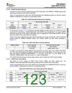
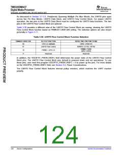
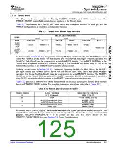
TMS320DM6437
Digital Media Processor
www.ti.com
SPRS345B–NOVEMBER 2006–REVISED MARCH 2007
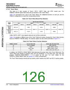
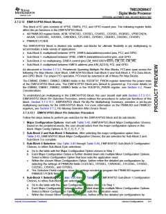
3.7.3.10 Serial Port Block
This block of 12 pins consists of McASP0, McBSP0, McBSP1, and GPIO muxed pins. The following
register fields select the pin functions in the Serial Port Block:
•
•
PINMUX1.SPBK0
PINMUX1.SPBK1
The Serial Port Block is further subdivided into these sub-blocks:
•
•
Serial Port Sub-Block 0: McBSP0, part of McASP0, GPIO.
Serial Port Sub-Block 1: McBSP1, part of McASP0, GPIO.
Table 3-35 summarizes the 12 pins in the Serial Port Block, the multiplexed function on each pin, and the
PINMUX configurations to select the corresponding function.
Table 3-35. Serial Port Block Muxed Pins Selection
MULTIPLEXED FUNCTIONS
SIGNAL NAME
McASP0
FUNCTION
McBSP0/1
FUNCTION
GPIO
SELECT
SELECT
FUNCTION
SELECT
Serial Port Sub-block 0
ACLKR0/CLKX0/GP[99]
AFSR0/DR0/GP[100]
ACLKR0
AFSR0
CLKX0
DR0
GP[99]
GP[100]
GP[101]
GP[102]
GP[103]
GP[104]
AHCLKR0/CLKR0/GP[101]
AXR0[3]/FSR0/GP[102]
AXR0[2]/FSX0/GP[103]
AXR0[1]/DX0/GP[104]
AHCLKR0
AXR0[3]
AXR0[2]
AXR0[1]
CLKR0
SPBK0 = 10
SPBK0 = 01
SPBK1 = 01
SPBK0 = 00
FSR0
FSX0
DX0
Serial Port Sub-block 1
AXR0[0]/FSR1/GP[105]
ACLKX0/CLKX1/GP[106]
AXR0[0]
ACLKX0
SPBK1 = 10/11
FSR1
GP[105]
GP[106]
SPBK1 =
01/11
SPBK1 = 10
CLKX1
AFSX0/DX1/GP[107]
SPBK1 =
01/11
AFSX0
AHCLKX0
AMUTEIN0
AMUTE0
SPBK1 = 10
SPBK1 = 10/11
SPBK1 = 10
DX1
CLKR1
FSX1
DR1
GP[107]
GP[108]
GP[109]
GP[110]
SPBK1 = 00
AHCLKX0/CLKR1/GP[108]
AMUTEIN0/FSX1/GP[109]
SPBK1 = 01
SPBK1 =
01/11
AMUTE0/DR1/GP[110]
SPBK1 = 10/11
SPBK1 = 01
As discussed in Section 3.7.3.2, Peripherals Spanning Multiple Pin Mux Blocks, the McBSP0 pins span
across two Pin Mux Blocks: Serial Port Sub-Block0, and Timer0 Block. For proper McBSP0 operation, the
Serial Port Sub-Block0 must be programmed to select McBSP0 function. The McBSP0 CLKS0 pin in the
Timer0 Block is optional for McBSP0 operation. CLKS0 is only needed if you desire using CLKS0 as an
external clock source to the McBSP0 internal sample rate generator.
Similarly, as discussed in Section 3.7.3.2, Peripherals Spanning Multiple Pin Mux Blocks, the McBSP1
pins span across two Pin Mux Blocks: Serial Port Sub-Block1, and Timer0 Block. For proper McBSP1
operation, the Serial Port Sub-Block1 must be programmed to select McBSP1 function. The McBSP1
CLKS1 pin in the Timer0 Block is optional for McBSP1 operation. CLKS1 is only needed if you desire
using CLKS1 as an external clock source to the McBSP1 internal sample rate generator.
Table 3-36 and Table 3-37 provide a different view of the Serial Port Block. Table 3-36 shows the Serial
Port Sub-Block 0 function based on PINMUX1.SPBK0 setting. Table 3-37 shows the Serial Port Sub-Block
1 function based on PINMUX1.SPBK1 setting. These selection options are also shown pictorially in
Figure 3-11.
Submit Documentation Feedback
Device Configurations
127

 TI [ TEXAS INSTRUMENTS ]