TMS320C6672
Multicore Fixed and Floating-Point Digital Signal Processor
SPRS708C—February 2012
www.ti.com
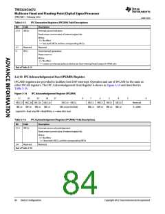
3.3.13 IPC Acknowledgement (IPCARx) Registers
IPCARx are the IPC interrupt-acknowledgement registers to facilitate inter-CorePac core interrupts.
The C6672 has two IPCARx registers (IPCAR0 through IPCAR1). These registers also provide a Source ID facility
by which up to 28 different sources of interrupts can be identified. Allocation of source bits to source processor and
meaning is entirely based on software convention. The register field descriptions are shown in the following tables.
Virtually anything can be a source for these registers as this is completely controlled by software. Any master that
has access to BOOTCFG module space can write to these registers. The IPC Acknowledgement Register is shown in
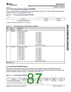
Figure 3-12 and described in Table 3-14.
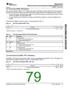
Figure 3-12
IPC Acknowledgement Registers (IPCARx)
31
30
29
28
27
8
7
6
5
4
3
0
SRCC27 SRCC26 SRCC25 SRCC24
RW +0 RW +0 RW +0 RW +0
SRCC23 – SRCC4
SRCC3
RW +0
SRCC2
RW +0
SRCC1
RW +0
SRCC0
RW +0
Reserved
R, +0000
RW +0 (per bit field)
Legend: R = Read only; RW = Read/Write; -n = value after reset
Table 3-14
IPC Acknowledgement Registers (IPCARx) Field Descriptions
Bit
Field
SRCCx
Description
31-4
Interrupt source acknowledgement.
Reads return current value of internal register bit.
Writes:
0 = No effect
1 = Clears both SRCCx and the corresponding SRCSx
3-0
Reserved
Reserved
End of Table 3-14
3.3.14 IPC Generation Host (IPCGRH) Register
IPCGRH register is provided to facilitate host DSP interrupt. Operation and use of IPCGRH is the same as
other IPCGR registers. Interrupt output pulse created by IPCGRH is driven on a device pin, host interrupt/event
output (HOUT).
The host interrupt output pulse should be stretched. It should be asserted for 4 bootcfg clock cycles (CPU/6)
followed by a deassertion of 4 bootcfg clock cycles. Generating the pulse will result in 8 CPU/6 cycle pulse blocking
window. Write to IPCGRH with IPCG bit (bit 0) set will only generate a pulse if they are beyond 8 CPU/6 cycle
period. The IPC Generation Host Register is shown in Figure 3-13 and described in Table 3-15.
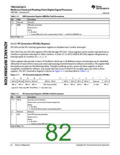
Figure 3-13
IPC Generation Registers (IPCGRH)
31
30
29
28
27
8
7
6
5
4
3
1
0
SRCS27 SRCS26 SRCS25 SRCS24
RW +0 RW +0 RW +0 RW +0
SRCS23 – SRCS4
SRCS3
RW +0
SRCS2
RW +0
SRCS1
RW +0
SRCS0
RW +0
Reserved
R, +000
IPCG
RW +0
RW +0 (per bit field)
Legend: R = Read only; RW = Read/Write; -n = value after reset
Copyright 2012 Texas Instruments Incorporated
Device Configuration 83

 TI [ TEXAS INSTRUMENTS ]