TMS320C6672
Multicore Fixed and Floating-Point Digital Signal Processor
SPRS708C—February 2012
www.ti.com
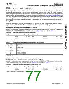
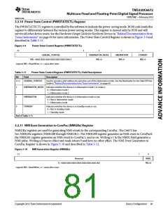
3.3.10 Power State Control (PWRSTATECTL) Register
The PWRSTATECTL register is controlled by the software to indicate the power-saving mode. ROM code reads this
register to differentiate between the various power saving modes. This register is cleared only by POR and will
survive all other device resets. See the Hardware Design Guide for KeyStone Devices in ‘‘Related Documentation from
Texas Instruments’’ on page 69 for more information. The Power State Control Register is shown in Figure 3-9 and
described in Table 3-11.
Figure 3-9
Power State Control Register (PWRSTATECTL)
31
3
2
1
0
GENERAL_PURPOSE
HIBERNATION_MODE
RW,+0
HIBERNATION
RW,+0
STANDBY
RW,+0
RW, +0000 0000 0000 0000 0000 0000 0000 0
Legend: RW = Read/Write; -n = value after reset
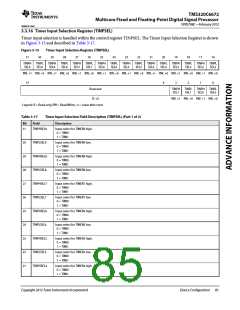
Table 3-11
Power State Control Register (PWRSTATECTL) Field Descriptions
Description
Bit
Field
31-3
GENERAL_PURPOSE
Used to provide a start address for execution out of the hibernation modes. See the Bootloader for the C66x DSP User
Guide in ‘‘Related Documentation from Texas Instruments’’ on page 69.
2
1
0
HIBERNATION_MODE Indicates whether the device is in hibernation mode 1 or mode 2.
0 = Hibernation mode 1
1 = Hibernation mode 2
HIBERNATION
STANDBY
Indicates whether the device is in hibernation mode or not.
0 = Not in hibernation mode
1 = Hibernation mode
Indicates whether the device is in standby mode or not.
0 = Not in standby mode
1 = Standby mode
End of Table 3-11
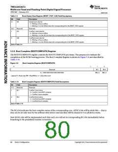
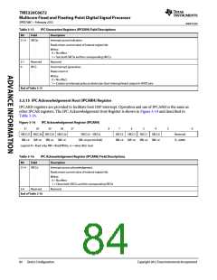
3.3.11 NMI Even Generation to CorePac (NMIGRx) Register
NMIGRx registers are used for generating NMI events to the corresponding CorePac. The C6672 has
two NMIGRx registers (NMIGR0 through NMIGR1). The NMIGR0 register generates an NMI event to CorePac0,
the NMIGR1 register generates an NMI event to CorePac1, and so on. Writing a 1 to the NMIG field generates a
NMI pulse. Writing a 0 has no effect and reads return 0 and have no other effect. The NMI Even Generation to
CorePac Register is shown in Figure 3-10 and described in Table 3-12.
Figure 3-10
NMI Generation Register (NMIGRx)
31
1
0
Reserved
R, +0000 0000 0000 0000 0000 0000 0000 000
NMIG
RW,+0
Legend: RW = Read/Write; -n = value after reset
Copyright 2012 Texas Instruments Incorporated
Device Configuration 81

 TI [ TEXAS INSTRUMENTS ]