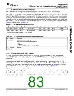
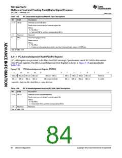
TMS320C6672
Multicore Fixed and Floating-Point Digital Signal Processor
SPRS708C—February 2012
www.ti.com
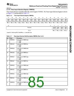
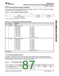
3.3.17 Timer Output Selection Register (TOUTPSEL)
The timer output selection is handled within the control register TOUTSEL. The Timer Output Selection Register
is shown in Figure 3-16 and described in Table 3-18.
Figure 3-16
Timer Output Selection Register (TOUTPSEL)
31
10
9
5
4
0
Reserved
TOUTPSEL1
RW,+00001
TOUTPSEL0
RW,+00000
R,+000000000000000000000000
Legend: R = Read only; RW = Read/Write; -n = value after reset
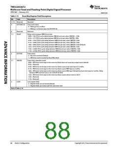
Table 3-18
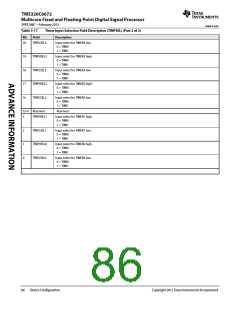
Timer Output Selection Field Description (TOUTPSEL)
Bit
Field
Description
31-10
9-5
Reserved
Reserved
TOUTPSEL1
Output select for TIMO1
00000: TOUTL0
00001: TOUTH0
00010: TOUTL1
00011: TOUTH1
10000: TOUTL2
10001: TOUTH2
10010: TOUTL3
10011: TOUTH3
10100: TOUTL4
10101: TOUTH4
10110: TOUTL5
10111: TOUTH5
11000: TOUTL6
11001: TOUTH6
11010: TOUTL7
11011: TOUTH7
11100: TOUTL8
11101: TOUTH8
11110: TOUTL9
11111: TOUTH9
00100 to 01111: Reserved
4-0
TOUTPSEL0
Output select for TIMO0
00000: TOUTL0
00001: TOUTH0
00010: TOUTL1
00011: TOUTH1
10000: TOUTL2
10001: TOUTH2
10010: TOUTL3
10011: TOUTH3
10100: TOUTL4
10101: TOUTH4
10110: TOUTL5
10111: TOUTH5
11000: TOUTL6
11001: TOUTH6
11010: TOUTL7
11011: TOUTH7
11100: TOUTL8
11101: TOUTH8
11110: TOUTL9
11111: TOUTH9
00100 to 01111: Reserved
End of Table 3-18
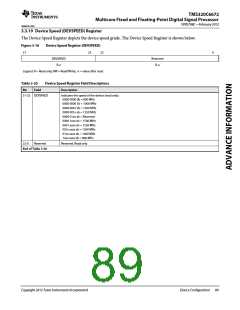
3.3.18 Reset Mux (RSTMUXx) Register
The software controls the Reset Mux block through the reset multiplex registers using RSTMUX0 through
RSTMUX1 for each of the two CorePacs on the C6672. These registers are located in Bootcfg memory space. The
Reset Mux Register is shown in Figure 3-17 and described in Table 3-19.
Figure 3-17
Reset Mux Register RSTMUXx
31
10
9
8
7
5
4
3
1
0
Reserved
R, +0000 0000 0000 0000 0000 00
EVTSTATCLR
RC, +0
Reserved
R, +0
DELAY
RW, +100
EVTSTAT
R, +0
OMODE
RW, +000
LOCK
RW, +0
Legend: R = Read only; RW = Read/Write; -n = value after reset; RC = Read only and write 1 to clear
Copyright 2012 Texas Instruments Incorporated
Device Configuration 87

 TI [ TEXAS INSTRUMENTS ]