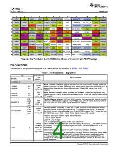
TLK10002
SLLSE75 –MAY 2011
www.ti.com
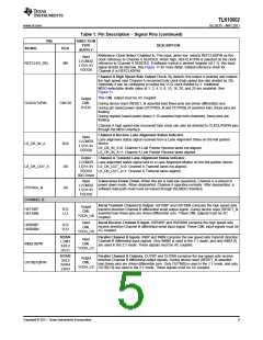
Table 1. Pin Description – Signal Pins (continued)
PIN
DIRECTION
TYPE
SUPPLY
DESCRIPTION
SIGNAL
BGA
JTAG Mode Select. TMS is used to control the state of the internal test-port controller. In
system applications where JTAG is not implemented, this input signal can be left
unconnected.
Input
LVCMOS
1.5V/1.8V
VDDO0
(Internal
Pullup)
TMS
TCK
B8
During pin based power down (PDTRXA_N and PDTRXB_N asserted low), this pin is not
pulled up.
During register based power down (1.15 asserted high both channels), this pin is pulled up.
Input
LVCMOS
with
Hysteresis
1.5V/1.8V
VDDO0
JTAG Clock. TCK is used to clock state information and test data into and out of the
device during boundary scan operation. In system applications where JTAG is not
implemented, this input signal should be grounded.
D8
E5
JTAG Test Reset. TRST_N is used to reset the JTAG logic into system operational mode.
This input can be left unconnected in the application and is pulled down internally, disabling
the JTAG circuitry. If JTAG is implemented on the application board, this signal should be
deasserted (high) during JTAG system testing, and otherwise asserted (low) during normal
operation mode.
Input
LVCMOS
1.5V/1.8V
VDDO0
TRST_N
During pin based power down (PDTRXA_N and PDTRXB_N asserted low), this pin is not
pulled down. During register based power down (1.15 asserted high both channels), this pin
is pulled down.
(Internal
Pulldown)
Input
Test Enable. This signal is used during the device manufacturing process. It should be
grounded through a resistor in the device application board. The application board should
allow the flexibility of easily reworking this signal to a high level if device debug is
necessary (by including an uninstalled resistor to VDDO).
LVCMOS
1.5V/1.8V
VDDO1
TESTEN
GPI0
L10
J10
Input
General Purpose Input Zero. This signal is used during the device manufacturing process.
It should be grounded through a resistor on the device application board. The application
board should also allow the flexibility of easily reworking this signal to a high level if device
debug is necessary (by including an uninstalled resistor to VDDO).
LVCMOS
1.5V/1.8V
VDDO1
SERDES Channel A Analog Testability I/O. This signal is used during the device
manufacturing process. It should be left unconnected in the device application.
AMUXA
AMUXB
C11
D4
Analog I/O
Analog I/O
SERDES Channel B Analog Testability I/O. This signal is used during the device
manufacturing process. It should be left unconnected in the device application.
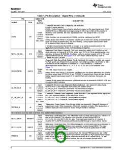
Table 2. Pin Description – Power Pins
PIN
Type
DESCRIPTION
SIGNAL
BGA
SERDES Analog Power. VDDA_LS and VDDA_HS provide supply voltage for the analog
Power circuits on the low-speed and high-speed sides respectively. 1.0V nominal. Can be tied
together on the application board.
D2, F2, G2,
J2 / F11, G10
VDDA_LS/HS
SERDES Analog Power. VDDT_LS and VDDT_HS provide termination and supply
Power voltage for the analog circuits on the low-speed and high-speed sides respectively. 1.0V
nominal. Can be tied together on the application board.
VDDT_LS/HS
F4, G4 / F9
E6, E8, F6, H6,
H8
SERDES Digital Power. VDDD provides supply voltage for the digital circuits internal to
the SERDES. 1.0V nominal.
VDDD
DVDD
Power
E7, F7, G6, G8,
H7
Power Digital Core Power. DVDD provides supply voltage to the digital core. 1.0V nominal.
SERDES Analog Regulator Power. VDDRA_LS and VDDRA_HS provide supply voltage
Power for the internal PLL regulator for Channel A low speed and high speed sides respectively.
1.5V or 1.8V nominal.
VDDRA_LS/HS
VDDRB_LS/HS
C3/E11
K3/J11
SERDES Analog Regulator Power. VDDRB_LS and VDDRB_HS provide supply voltage
Power for the internal PLL regulator for Channel B low speed and high speed sides respectively.
1.5V or 1.8V nominal.
LVCMOS I/O Power. VDDO0 and VDDO1 provide supply voltage for the LVCMOS inputs
Power
VDDO[1:0]
VPP
K7/C7
D7
and outputs. 1.5V or 1.8V nominal. Can be tied together on the application board.
Factory Program Voltage. Used during device manufacturing. The application must
Power
connect this power supply directly to DVDD.
8
Copyright © 2011, Texas Instruments Incorporated

 TI [ TEXAS INSTRUMENTS ]