TLK10002
www.ti.com
SIGNAL
SLLSE75 –MAY 2011
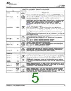
Table 1. Pin Description – Signal Pins (continued)
PIN
DIRECTION
TYPE
DESCRIPTION
BGA
SUPPLY
Receive PRBS Error Free (Pass) Indicator.
When PRBS test is enabled (PRBSEN=1): PRBS_PASS=1 indicates that PRBS pattern
reception is error free. PRBS_PASS=0 indicates that a PRBS error is detected. The
channel, high speed or low speed side, and lane (for low speed side) that this signal refers
to is chosen through MDIO register bits 0.3:0.
Output
LVCMOS
1.5V/1.8V
VDDO1
During device reset (RESET_N asserted low) this pin is driven low.
During pin based power down (PDTRXA_N and PDTRXB_N asserted low), this pin is
floating.
PRBS_PASS
J9
40Ω Driver
During register based power down, this pin is floating.
It is highly recommended that PRBS_PASS be brought to easily accessible point on the
application board (header), in the event that debug is required.
MDIO Port Address. Used to select the MDIO port address.
PRTAD[4:1] selects the MDIO port address. The TLK10002 has two different MDIO port
addresses. Selecting a unique PRTAD[4:1] per TLK10002 device allows 16 TLK10002
devices per MDIO bus. Each channel can be accessed by setting the appropriate port
address field within the serial interface protocol transaction.
M8
J6
L9
G9
E10
Input
LVCMOS
1.5V/1.8V
VDDO[1:0]
The TLK10002 will respond if the 4 MSB’s of the port address field on MDIO protocol
(PA[4:1]) matches PRTAD[4:1]. The LSB of port address field (PA[0]) determines which
TLK10002 channel responds. Channel A responds when PA[0]=0 and Channel B responds
when PA[0]=1.
PRTAD[4:0]
PRTAD[0] is not used functionally, but is present for device testability and compatibility with
other devices in the family of products. PRTAD[0] should be grounded on the application
board.
Input
Low True Device Reset. RESET_N must be held asserted (low logic level) for at least 10
µs after device power stabilization.
LVCMOS
1.5V/1.8V
VDDO1
RESET_N
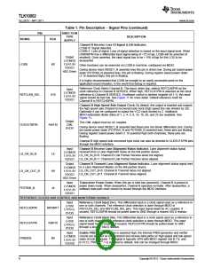
MDC
H5
J8
Input
MDIO Clock Input. Clock input for the Clause 22 MDIO interface.
LVCMOS Note that an external pullup is generally not required on MDC.
with
Hysteresis
1.5V/1.8V
VDDO1
MDIO Data I/O. MDIO interface data input/output signal for the Clause 22 MDIO interface.
This signal must be externally pulled up to VDDO, using a 2kΩ resistor.
Input/Output
During device reset (RESET_N asserted low) this pin is floating. During register based
power down the management interface remains active for control register writes and reads.
Certain status bits are not deterministic as their generating clock source may be disabled
as a result of asserting either power down input signal. During pin based power down
(PDTRXA_N and PDTRXB_N asserted low), this pin is floating. During register based
power down (1.15 asserted high both channels), this pin is driven normally.
LVCMOS
1.5V/1.8V
VDDO1
MDIO
J7
25Ω Driver
Input
JTAG Input Data. TDI is used to serially shift test data and test instructions into the device
during the operation of the test port. In system applications where JTAG is not
implemented, this input signal may be left floating.
LVCMOS
1.5V/1.8V
VDDO0
(Internal
Pullup)
TDI
C8
D6
During pin based power down (PDTRXA_N and PDTRXB_N asserted low), this pin is not
pulled up. During register based power down (1.15 asserted high both channels), this pin is
pulled up.
JTAG Output Data. TDO is used to serially shift test data and test instructions out of the
device during operation of the test port. When the JTAG port is not in use, TDO is in a high
impedance state.
Output
LVCMOS
1.5V/1.8V
VDDO0
TDO
During device reset (RESET_N asserted low) this pin is floating.
During pin based power down (PDTRXA_N and PDTRXB_N asserted low), this pin is
floating.
50Ω Driver
During register based power down (1.15 asserted high both channels), this pin is floating.
Copyright © 2011, Texas Instruments Incorporated
7

 TI [ TEXAS INSTRUMENTS ]