TLK10002
SLLSE75 –MAY 2011
www.ti.com
1
2
3
4
5
6
7
8
9
10
11
12
A
B
INA1P
INA1N
VSS
VSS
INA2P
INA0N
INA0P
VSS
OUTA0P OUTA0N PDTRXA_N
CLKOUTBP
CLKOUTBN
VSS
HSRXAN
VSS
VSS
OUTA1P OUTA1N
VSS
VDDO0
VPP
TMS
TDI
PRBSEN
CLKOUTAP
LS_OK_OUT_A
LOSA
LS_OK_IN_A
CLKOUTAN
VSS
VSS
AMUXA
VSS
HSRXAP
VSS
C
D
E
INA2N
VDDRA_LS OUTA2P OUTA2N
VSS
TDO
INA3P
INA3N
VSS
VDDA_LS
VSS
VSS
AMUXB
VSS
VSS
TCK
HSTXAP
OUTA3N
TRST_N VDDD
DVDD
DVDD
VSS
VDDD
VSS
PRTAD0
VSS
VDDRA_HS HSTXAN
F
VDDA_LS
VDDA_LS
VSS
OUTA3P VDDT_LS
VSS
VSS
VDDD
DVDD
VDDT_HS
PRTAD1
VDDA_HS
VSS
VSS
G
H
J
VSS
VSS
VDDT_LS
VSS
DVDD
VDDD
MDC
VDDA_HS
HSRXBN
HSRXBP
VSS
INB0P
INB0N
VSS
OUTB0N
RESET_N VDDD
DVDD
MDIO
VDDO1
VSS
LS_OK_OUT_B REFCLKB_SEL
VSS
VDDA_LS
INB1P
OUTB0P PDTRXB_N VSS
PRTAD3
VSS
PRBS_PASS
REFCLK1P
PRTAD2
GPI0
VDDRB_HS
VSS
K
L
VDDRB_LS OUTB1N OUTB1P
LOSB
REFCLK1N
TESTEN
HSTXBP
HSTXBN
VSS
INB2P
INB2N
INB1N
VSS
VSS
OUTB2N OUTB2P
VSS
LS_OK_IN_B
VSS
M
VSS
INB3P
INB3N
OUTB3N OUTB3P
PRTAD4 REFCLKA_SEL REFCLK0P REFCLK0N
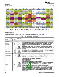
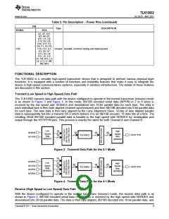
Figure 2. The Pin-Out of the TLK10002 in a 13-mm x 13-mm 144-pin PBGA Package
PIN FUNCTIONS
The details of the pin functions of the TLK10002 device are provided in Table 1 and Table 2.
Table 1. Pin Description – Signal Pins
PIN
DIRECTION
TYPE
SUPPLY
DESCRIPTION
SIGNAL
BGA
CHANNEL A
Serial Transmit Channel A Output. HSTXAP and HSTXAN comprise the high speed side
transmit direction Channel A differential serial output signal. During device reset (RESET_N
asserted low) these pins are driven differential zero. These CML outputs must be AC
coupled.
Output
CML
VDDA_HS
HSTXAP
HSTXAN
D12
E12
Input
CML
VDDA_HS
Serial Receive Channel A Input. HSRXAP and HSRXAN comprise the high speed side
receive direction Channel A differential serial input signal. These CML input signals must be
AC coupled.
HSRXAP
HSRXAN
B12
A12
D1/E1
B2/C2
A1/B1
A4/A3
Parallel Channel A Inputs. INAP and INAN comprise the low speed side transmit direction
Channel A differential input signals. Only INA[0] is used in the 1:1 mode, and only INA[1:0]
are used in the 2:1 mode. These signals must be AC coupled.
Input
CML
VDDA_LS
INA[3:0]P/N
F3/E3
C4/C5
B5/B6
A6/A7
Parallel Channel A Outputs. OUTAP and OUTAN comprise the low speed side receive
direction Channel A differential output signals. During device reset (RESET_N asserted
low) these pins are driven differential zero. Only OUTA[0] is used in the 1:1 mode, and only
OUTA[1:0] are used in the 2:1 mode. These signals must be AC coupled.
Output
CML
VDDA_LS
OUTA[3:0]P/N
Channel A Receive Loss Of Signal (LOS) Indicator.
LOSA=0: Signal detected.
LOSA=1: Loss of signal.
Loss of signal detection is based on the input signal level.
When HSRXAP/N has a differential input signal swing of <75 mVpp, LOSA will be asserted
(if enabled). Once asserted, the input signal has to be > 150 mVpp for this LOS to be
deasserted.
Output
LVCMOS
1.5V/1.8V
VDDO0
LOSA
E9
Other functions can be observed on LOSA in real-time, configured via MDIO.
40Ω Driver
During device reset (RESET_N asserted low) this pin is driven low. During pin based power
down (PDTRXA_N asserted low), this pin is floating. During register based power down
(1.15 asserted high), this pin is floating. NOTE: It is highly recommended that LOSA be
brought to an easily accessible point on the application board (header), in the event that
debug is required.
4
Copyright © 2011, Texas Instruments Incorporated

 TI [ TEXAS INSTRUMENTS ]