TLK10002
www.ti.com
SIGNAL
SLLSE75 –MAY 2011
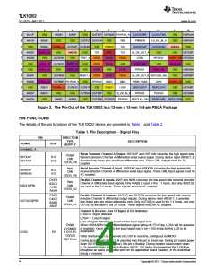
Table 1. Pin Description – Signal Pins (continued)
PIN
DIRECTION
TYPE
DESCRIPTION
BGA
SUPPLY
Reference Clock Select Channel A. This input, when low, selects REFCLK0P/N as the
clock reference to Channel A SERDES. When high, REFCLK1P/N is selected as the clock
reference to Channel A SERDES. If software control is desired (register bit 1.1), this input
signal should be tied low. See Figure 11 for more detail. Default reference clock for
Channel A is REFCLK0P/N.
Input
LVCMOS
1.5V/1.8V
VDDO0
REFCLKA_SEL
M9
Channel A High Speed Side Output Clock. By default, this output is enabled and outputs
the high speed side Channel A recovered byte clock (high speed line rate divided by 20).
Optionally it can be configured to output the VCO clock divided by 2. Additional
MDIO-selectable divide ratios of 1, 2, 4, 5, 8, 10, 16, 20, and 25 are available. See
Figure 11.
This CML output must be AC coupled.
Output
CML
CLKOUTAP/N
C9/C10
During device reset (RESET_N asserted low) these pins are driven differential zero.
DVDD
During pin based power down (PDTRXA_N and PDTRXB_N asserted low), these pins are
floating.
During register based power down (1.15 asserted high both channels), these pins are
floating.
Channel A high speed side recovered byte clock can also be directed to CLKOUTBP/N pins
through the MDIO interface.
Channel A Receive Lane Alignment Status Indicator.
Lane alignment status signal received from a Lane Alignment Slave on the link partner
device.
LS_OK_IN_A=0: Channel A Link Partner Receive lanes not aligned.
LS_OK_IN_A=1: Channel A Link Partner Receive lanes aligned
Input
LVCMOS
1.5V/1.8V
VDDO0
LS_OK_IN_A
B10
Output
Channel A Transmit Lane Alignment Status Indicator.
LVCMOS Lane alignment status signal sent to a Lane Alignment Master on the link partner device.
1.5V/1.8V LS_OK_OUT_A=0: Channel A Transmit lanes not aligned.
LS_OK_OUT_A
D9
A8
VDDO0
LS_OK_OUT_A=1: Channel A Transmit lanes aligned.
40Ω Driver
Input
Transceiver Power Down. When this pin is held low (asserted), Channel A is placed in
power down mode. When deasserted, Channel A operates normally. After deassertion, a
software data path reset must be issued through the MDIO interface.
LVCMOS
1.5V/1.8V
VDDO0
PDTRXA_N
CHANNEL B
Serial Transmit Channel B Output. HSTXBP and HSTXBN comprise the high speed side
transmit direction Channel B differential serial output signal. During device reset (RESET_N
asserted low) these pins are driven differential zero. These CML outputs must be AC
coupled.
Output
CML
VDDA_HS
HSTXBP
HSTXBN
K12
L12
Input
CML
VDDA_HS
Serial Receive Channel B Input. HSRXBP and HSRXBN comprise the high speed side
receive direction Channel B differential serial input signal. These CML input signals must be
AC coupled.
HSRXBP
HSRXBN
H12
G12
M3/M4
L1/M1
K2/L2
H1/J1
Parallel Channel B Inputs. INBP and INBN comprise the low speed side transmit direction
Channel B differential input signals. Only INB[0] is used in the 1:1 mode, and only INB[1:0]
are used in the 2:1 mode. These signals must be AC coupled.
Input
CML
VDDA_LS
INB[3:0]P/N
M7/M6
L6/L5
K5/K4
J3/H3
Parallel Channel B Outputs. OUTBP and OUTBN comprise the low speed side receive
direction Channel B differential output signals. During device reset (RESET_N asserted
low) these pins are driven differential zero. Only OUTB[0] is used in the 1:1 mode, and only
OUTB[1:0] are used in the 2:1 mode. These signals must be AC coupled.
Output
CML
VDDA_LS
OUTB[3:0]P/N
Copyright © 2011, Texas Instruments Incorporated
5

 TI [ TEXAS INSTRUMENTS ]