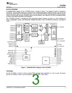
TLK10002
SLLSE75 –MAY 2011
www.ti.com
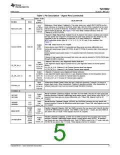
Table 1. Pin Description – Signal Pins (continued)
PIN
DIRECTION
TYPE
SUPPLY
DESCRIPTION
SIGNAL
BGA
Channel B Receive Loss Of Signal (LOS) Indicator.
LOSB=0: Signal detected.
LOSB=1: Loss of signal. Loss of signal detection is based on the input signal level. When
HSRXBP/N has a differential input signal swing of <75 mVpp, LOSB will be asserted (if
enabled). Once asserted, the input signal has to be > 150 mVpp for this LOS to be
deasserted
Output
LVCMOS
1.5V/1.8V
VDDO1
LOSB
K8
Other functions can be observed on LOSB in real-time, configured via MDIO.
During device reset (RESET_N asserted low) this pin is driven low. During pin based power
down (PDTRXB_N asserted low), this pin is floating. During register based power down
(1.15 asserted high), this pin is floating.
40Ω Driver
It is highly recommended that LOSB be brought to an easily accessible point on the
application board (header), in the event that debug is required.
Reference Clock Select Channel B. This input, when low, selects REFCLK0P/N as the
clock reference to Channel B SERDES. When high, REFCLK1P/N is selected as the clock
reference to Channel B SERDES. If software control is desired (register bit 1.1), this input
signal should be tied low. See Figure 11 for more detail. Default reference clock for
Channel B is REFCLK0P/N.
Input
LVCMOS
1.5V/1.8V
VDDO1
REFCLKB_SEL
H10
Channel B High Speed Side Output Clock. By default, this output is enabled and outputs
the high speed side Channel B recovered byte clock (high speed line rate divided by 20).
Optionally it can be configured to output the VCO clock divided by 2. Additional
MDIO-selectable divide ratios of 1, 2, 4, 5, 8, 10, 16, 20, and 25 are available. See
Figure 11.
Output
CML
DVDD
This CML output must be AC coupled.
CLKOUTBP/N
A9/A10
During device reset (RESET_N asserted low) these pins are driven differential zero. During
pin based power down (PDTRXA_N and PDTRXB_N asserted low), these pins are floating.
During register based power down (1.15 asserted high both channels), these pins are
floating.
Channel B high speed side recovered byte clock can also be directed to CLKOUTAP/N pins
through the MDIO interface.
Input
Channel B Receive Lane Alignment Status Indicator. Lane alignment status signal
received from a Lane Alignment Slave on the link partner device.
LS_OK_IN_B=0: Channel B Link Partner Receive lanes not aligned.
LS_OK_IN_B=1: Channel B Link Partner Receive lanes aligned
LVCMOS
1.5V/1.8V
VDDO1
LS_OK_IN_B
LS_OK_OUT_B
PDTRXB_N
L8
H9
J4
Output
LVCMOS
1.5V/1.8V
VDDO1
Channel B Transmit Lane Alignment Status Indicator. Lane alignment status signal sent
to a Lane Alignment Master on the link partner device.
LS_OK_OUT_B=0: Channel B Transmit lanes not aligned.
LS_OK_OUT_B=1: Channel B Transmit lanes aligned.
40Ω Driver
Input
Transceiver Power Down. When this pin is held low (asserted), Channel B is placed in
power down mode. When deasserted, Channel B operates normally. After deassertion, a
software data path reset should be issued through the MDIO interface.
LVCMOS
1.5V/1.8V
VDDO1
REFERENCE CLOCKS AND CONTROL AND MONITORING SIGNALS
Input
LVDS/
LVPECL
DVDD
Reference Clock Input Zero. This differential input is a clock signal used as a reference to
one or both channels. The reference clock selection is done through MDIO or
REFCLKA_SEL and REFCLKB_SEL pins. This input signal must be AC coupled. If
unused, REFCLK0P/N should be pulled down to GND through a shared 100 Ω resistor.
REFCLK0P/N
REFCLK1P/N
PRBSEN
M10/M11
K9/K10
B9
Input
LVDS/
LVPECL
DVDD
Reference Clock Input One. This differential input is a clock signal used as a reference to
one or both channels. The reference clock selection is done through MDIO. This input
signal must be AC coupled. If unused, REFCLK1P/N should be pulled down to GND
through a shared 100 Ω resistor.
Input
Enable PRBS: When this pin is asserted high, the internal PRBS generator and verifier
circuits are enabled on both transmit and receive data paths on high speed and low speed
sides of both channels. This signal is logically OR’d with MDIO register bits B.7:6, and
B.13:12. PRBS 231-1 is selected by default, and can be changed through MDIO.
LVCMOS
1.5V/1.8V
VDDO0
6
Copyright © 2011, Texas Instruments Incorporated

 TI [ TEXAS INSTRUMENTS ]