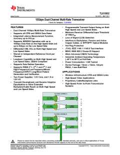
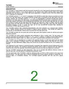
TLK10002
www.ti.com
SLLSE75 –MAY 2011
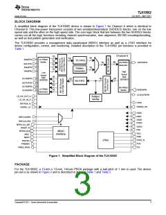
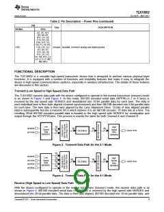
BLOCK DIAGRAM
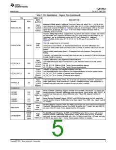
A simplified block diagram of the TLK10002 device is shown in Figure 1 for Channel A which is identical to
Channel B. This low-power transceiver consists of two serializer/deserializer (SERDES) blocks, one on the low
speed side and the other on the high speed side. The core logic block that lies between the two SERDES blocks
carries out all the logic functions including channel synchronization, lane alignment, 8B/10B encoding/decoding,
as well as test pattern generation and verification.
The TLK10002 provides a management data input/output (MDIO) interface as well as a JTAG interface for
device configuration, control, and monitoring. Detailed description of the TLK10002 pin functions is provided in
Table 1.
Ch annel A
10
16
16
32
INA0P/N
LS PRBS
Verifier
TX FIFO
10
10
20
20
HS PRBS
Generator
HSTXAP/N
16
INA1P/N
INA2P/N
INA3P/N
Pattern
Generator
10
High
Speed
Side
Low
Speed
Side
10
OUTA0P/N
16
32
SERDES
SERDES
RX FIFO
10
10
OUTA1P/N
OUTA2P/N
OUTA3P/N
HS PRBS
Verifier
LS PRBS
Generator
10
HSRXAP/N
CLKOUTAP/N
LS_OK_OUT_A
LS_OK_IN_A
Pattern
Verifier
LOSA
PDTRXA_N
VDDRA_LS
VDDRA_HS
VDDA
VDDT
VDDD
DVDD
REFCLK0P/N
REFCLK1P/N
REFCLKA_SEL
RESET_N
PRTAD [4:0]
MDC
VDDO
VSS
MDIO
Interface
TDO
TMS
MDIO
TRST_N
JTAG
TESTEN
PRBSEN
TCK
TDI
PRBS_PASS
Figure 1. Simplified Block Diagram of the TLK10002
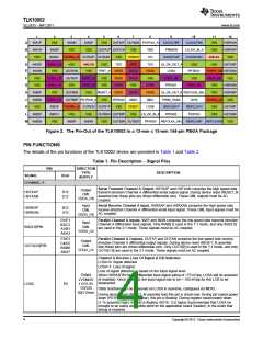
PACKAGE
For the TLK10002, a 13-mm x 13-mm, 144-pin PBGA package with a ball pitch of 1 mm is used. The device
pin-out is as shown in Figure 2 and is described in detail in Table 1 and Table 2.
Copyright © 2011, Texas Instruments Incorporated
3

 TI [ TEXAS INSTRUMENTS ]