THS4631
www.ti.com
SLOS451A–DECEMBER 2004–REVISED MARCH 2005
SUMMARY OF KEY DECISIONS IN
TRANSIMPEDANCE DESIGN
feedback resistors this large or anticipate using an
external compensation scheme to stabilize the circuit.
Using a simple capacitor in parallel with the feedback
resistor makes the amplifier more stable as shown in
the Typical Characteristics graphs.
The following is a simplified process for basic
transimpedance circuit design. This process gives a
start to the design process, though it does ignore
some aspects that may be critical to the circuit.
NOISE ANALYSIS
STEP 1:
Determine the capacitance of the
source.
High slew rate, unity gain stable, voltage-feedback
operational amplifiers usually achieve their slew rate
at the expense of a higher input noise voltage. The
7 nV/√Hz input voltage noise for the THS4631 is,
however, much lower than comparable amplifiers
while achieving high slew rates. The input-referred
voltage noise, and the input-referred current noise
term, combine to give low output noise under a wide
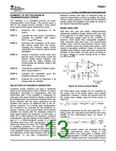
variety of operating conditions. Figure 42 shows the
amplifier noise analysis model with all the noise terms
included. In this model, all noise terms are taken to
be noise voltage or current density terms in either
nV/√Hz or fA/√Hz.
STEP 2:
Calculate the total source capacitance,
including the amplifier input capaci-
tance, CI(CM) and CI(DIFF)
.
STEP 3:
STEP 4:
Determine the magnitude of the poss-
ible current output from the source,
including the minimum signal current
anticipated and maximum signal current
anticipated.
Choose a feedback resistor value such
that the input current levels create the
desired output signal voltages, and
ensure that the output voltages can
accommodate the dynamic range of the
input signal.
E
NI
+
_
E
O
R
S
I
BN
STEP 5:
STEP 6:
STEP 7:
Calculate the optimum feedback capaci-
tance using Equation 1.
E
RF
E
RS
4kTR
R
I
S
f
Calculate the bandwidth given the
resulting component values.
R
g
4kT
4kTR
f
BI
R
g
Evaluate the circuit to determine if all
design goals are satisfied.
4kT = 1.6E−20J
at 290K
SELECTION OF FEEDBACK RESISTORS
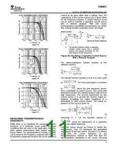
Figure 42. Noise Analysis Model
Feedback resistor selection can have a significant
effect on the performance of the THS4631 in a given
application, especially in configurations with low
closed-loop gain. If the amplifier is configured for
unity gain, the output should be directly connected to
the inverting input. Any resistance between these two
points interacts with the input capacitance of the
amplifier and causes an additional pole in the fre-
quency response. For nonunity gain configurations,
low resistances are desirable for flat frequency re-
sponse. However, care must be taken not to load the
amplifier too heavily with the feedback network if
large output signals are expected. In most cases, a
trade off is made between the frequency response
characteristics and the loading of the amplifier. For a
gain of 2, a 499-Ω feedback resistor is a suitable
operating point from both perspectives. If resistor
values are chosen too large, the THS4631 is subject
to oscillation problems. For example, an inverting
amplifier configuration with a 5-kΩ gain resistor and a
5-kΩ feedback resistor develops an oscillation due to
the interaction of the large resistors with the input
capacitance. In low gain configurations, avoid
The total output noise voltage can be computed as
the square root of all square output noise voltage
contributors. Equation 7 shows the general form for
the output noise voltage using the terms shown in
Figure 42.
2
2
ǒ
SǓ2 Ǔ2
ǒ
) 4kTRS NG ) IBIRf ) 4kTRfNG
+ Ǹǒ
Ǔ
EO
ENI ) IBN
R
(7)
Dividing this expression by the noise gain [NG = (1+
Rf/Rg)] gives the equivalent input-referred spot noise
voltage at the noninverting input, as shown in
Equation 8:
2
IBIRf
4kTRf
NG
2
ǒ
SǓ2
) 4kTRS )
Ǹ
ǒ Ǔ )
NG
EN +
ENI ) IBN
R
(8)
Using high resistor values can dominate the total
equivalent input-referred noise. Using 3-kΩ
a
source-resistance (RS) value adds a voltage noise
term of approximately 7 nV/√Hz. This is equivalent to
the amplifier voltage noise term. Using higher resistor
13

 TI [ TEXAS INSTRUMENTS ]