THS4631
www.ti.com
SLOS451A–DECEMBER 2004–REVISED MARCH 2005
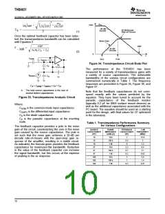
values dominate the noise of the system. Although
the THS4631 JFET input stage is ideal for
high-source impedance because of the low-bias cur-
rents, the system noise and bandwidth is limited by a
high-source (RS) impedance.
formance of the THS4631. Resistors should be a
very low reactance type. Surface-mount resistors
work best and allow a tighter overall layout.
Again, keep their leads and PC board trace
length as short as possible. Never use wirebound
type resistors in a high frequency application.
Since the output pin and inverting input pins are
the most sensitive to parasitic capacitance,
always position the feedback and series output
resistors, if any, as close as possible to the
inverting input pins and output pins. Other net-
work components, such as input termination re-
sistors, should be placed close to the gain-setting
resistors. Even with a low parasitic capacitance
shunting the external resistors, excessively high
resistor values can create significant time con-
stants that can degrade performance. Good axial
metal-film or surface-mount resistors have ap-
proximately 0.2 pF in shunt with the resistor. For
resistor values > 2.0 kΩ, this parasitic capaci-
tance can add a pole and/or a zero that can
effect circuit operation. Keep resistor values as
low as possible, consistent with load driving
considerations.
SLEW RATE PERFORMANCE WITH VARYING
INPUT STEP AMPLITUDE AND RISE/FALL
TIME
Some FET input amplifiers exhibit the peculiar
behavior of having a larger slew rate when presented
with smaller input voltage steps and slower edge
rates due to a change in bias conditions in the input
stage of the amplifier under these circumstances.
This phenomena is most commonly seen when FET
input amplifiers are used as voltage followers. As this
behavior is typically undesirable, the THS4631 has
been designed to avoid these issues. Larger ampli-
tudes lead to higher slew rates, as would be antici-
pated, and fast edges do not degrade the slew rate of
the device. The high slew rate of the THS4631 allows
improved SFDR and THD performance, especially
noticeable above 5 MHz.
•
Connections to other wideband devices on the
board may be made with short direct traces or
through onboard transmission lines. For short
connections, consider the trace and the input to
the next device as a lumped capacitive load.
Relatively wide traces (50 mils to 100 mils)
should be used, preferably with ground and
power planes opened up around them. Estimate
the total capacitive load and determine if isolation
resistors on the outputs are necessary. Low
parasitic capacitive loads (< 4 pF) may not need
an RS since the THS4631 is nominally compen-
sated to operate with a 2-pF parasitic load.
Higher parasitic capacitive loads without an RS
are allowed as the signal gain increases
(increasing the unloaded phase margin). If a long
trace is required, and the 6-dB signal loss intrin-
sic to a doubly-terminated transmission line is
acceptable, implement a matched impedance
transmission line using microstrip or stripline
techniques (consult an ECL design handbook for
microstrip and stripline layout techniques). A
50-Ω environment is not necessary onboard, and
in fact, a higher impedance environment im-
proves distortion as shown in the distortion ver-
sus load plots. With a characteristic board trace
impedance based on board material and trace
dimensions, a matching series resistor into the
trace from the output of the THS4631 is used as
well as a terminating shunt resistor at the input of
the destination device. Remember also that the
terminating impedance is the parallel combination
of the shunt resistor and the input impedance of
the destination device: this total effective im-
pedance should be set to match the trace im-
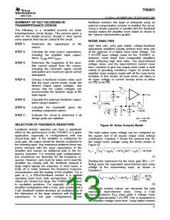
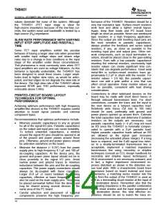
PRINTED-CIRCUIT BOARD LAYOUT
TECHNIQUES FOR OPTIMAL
PERFORMANCE
Achieving optimum performance with high frequency
amplifier-like devices in the THS4631 requires careful
attention to board layout parasitic and external
component types.
Recommendations that optimize performance include:
•
Minimize parasitic capacitance to any ac ground
for all of the signal I/O pins. Parasitic capacitance
on the output and input pins can cause instability.
To reduce unwanted capacitance, a window
around the signal I/O pins should be opened in all
of the ground and power planes around those
pins. Otherwise, ground and power planes should
be unbroken elsewhere on the board.
•
Minimize the distance (< 0.25”) from the power
supply pins to high frequency 0.1-µF and 100-pF
de-coupling capacitors. At the device pins, the
ground and power plane layout should not be in
close proximity to the signal I/O pins. Avoid
narrow power and ground traces to minimize
inductance between the pins and the de-coupling
capacitors. The power supply connections should
always be de-coupled with these capacitors.
Larger (6.8 µF or more) tantalum de-coupling
capacitors, effective at lower frequency, should
also be used on the main supply pins. These may
be placed somewhat farther from the device and
may be shared among several devices in the
same area of the PC board.
•
Careful selection and placement of external
components preserve the high frequency per-
14

 TI [ TEXAS INSTRUMENTS ]