THS4631
www.ti.com
SLOS451A–DECEMBER 2004–REVISED MARCH 2005
APPLICATION INFORMATION
The large gain-bandwidth product of the THS4631
provides the capability for simultaneously achieving
both high-transimpedance gain, wide bandwidth, high
slw rate, and low noise. In addition, the high-power
supply rails provide the potential for a very wide
dynamic range at the output, allowing for the use of
input sources which possess wide dynamic range.
The combination of these characteristics makes the
THS4631 a design option for systems that require
transimpedance amplification of wideband, low-level
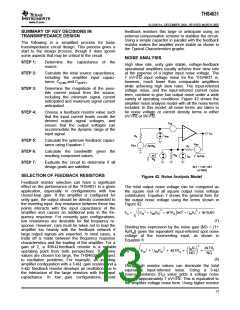
input signals. A standard transimpedance circuit is
shown in Figure 32.
INTRODUCTION
The THS4631 is a high-speed, FET-input operational
amplifier. The combination of: high gain bandwidth
product of 210 MHz, high slew rate of 1000 V/µs, and
trimmed dc precision makes the device an excellent
design option for a wide variety of applications,
including test and measurement, optical monitoring,
transimpedance gain circuits, and high-impedance
buffers. The applications section of the data sheet
discusses these particular applications in addition to
general information about the device and its features
Photodiode Circuit
TRANSIMPEDANCE FUNDAMENTALS
C
F
F
FET-input
amplifiers
are
often
used
in
transimpedance applications because of their ex-
tremely high input impedance. A transimpedance
block accepts a current as an input and converts this
current to a voltage at the output. The high-input
impedance associated with FET-input amplifiers
minimizes errors in this process caused by the input
bias currents, IIB, of the amplifier.
R
_
+
λ
R
L
−V
(Bias)
DESIGNING THE TRANSIMPEDANCE
CIRCUIT
Figure 32. Wideband Photodiode Transimpedance
Amplifier
Typically, design of a transimpedance circuit is driven
by the characteristics of the current source that
provides the input to the gain block. A photodiode is
the most common example of a capacitive current
source that interfaces with a transimpedance gain
block. Continuing with the photodiode example, the
system designer traditionally chooses a photodiode
based on two opposing criteria: speed and sensitivity.
Faster photodiodes cause a need for faster gain
stages, and more sensitive photodiodes require
higher gains in order to develop appreciable signal
levels at the output of the gain stage.
As indicated, the current source typically sets the
requirements for gain, speed, and dynamic range of
the amplifier. For a given amplifier and source combi-
nation, achievable performance is dictated by the
following parameters: the amplifier gain-bandwidth
product, the amplifier input capacitance, the source
capacitance, the transimpedance gain, the amplifier
slew rate, and the amplifier output swing. From this
information, the optimal performance of
a
transimpedance circuit using a given amplifier is
determined. Optimal is defined here as providing the
required transimpedance gain with a maximized flat
frequency response.
These parameters affect the design of the
transimpedance circuit in a few ways. First, the speed
of the photodiode signal determines the required
bandwidth of the gain circuit. Second, the required
gain, based on the sensitivity of the photodiode, limits
the bandwidth of the circuit. Third, the larger capaci-
tance associated with a more sensitive signal source
also detracts from the achievable speed of the gain
block. The dynamic range of the input signal also
places requirements on the amplifier dynamic range.
Knowledge of the source output current levels,
coupled with a desired voltage swing on the output,
dictates the value of the feedback resistor, RF. The
transfer function from input to output is VOUT = IINRF.
For the circuit shown in Figure 32, all but one of the
design parameters is known; the feedback capacitor
(CF) must be determined. Proper selection of the
feedback capacitor prevents an unstable design,
controls pulse response characteristics, provides
maximized flat transimpedance bandwidth, and limits
broadband integrated noise. The maximized flat fre-
quency response results with CF calculated as shown
in Equation 1, where CF is the feedback capacitor, RF
is the feedback resistor, CS is the total source
capacitance (including amplifier input capacitance
and parasitic capacitance at the inverting node), and
GBP is the gain-bandwidth product of the amplifier in
hertz.
9

 TI [ TEXAS INSTRUMENTS ]