THS4631
www.ti.com
SLOS451A–DECEMBER 2004–REVISED MARCH 2005
pedance. If the 6-dB attenuation of a doubly
terminated transmission line is unacceptable, a
long trace can be series-terminated at the source
end only. Treat the trace as a capacitive load in
this case. This does not preserve signal integrity
or a doubly-terminated line. If the input im-
pedance of the destination device is low, there is
some signal attenuation due to the voltage divider
formed by the series output into the terminating
impedance.
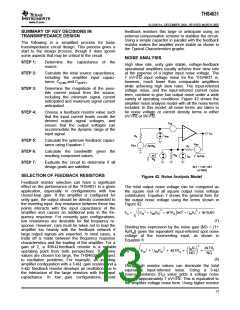
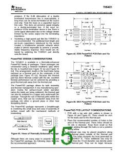
0.205
0.060
0.017
Pin 1
0.013
0.030
0.075
0.025 0.094
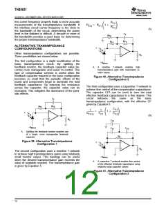
•
Socketing a high-speed part like the THS4631 is
not recommended. The additional lead length and
pin-to-pin capacitance introduced by the socket
creates a troublesome parasitic network which
makes it almost impossible to achieve a smooth,
stable frequency response. Best results are ob-
tained by soldering the THS4631 part directly
onto the board.
0.035
0.040
0.010
vias
Top View
Figure 44. DGN PowerPAD PCB Etch and Via
Pattern
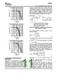
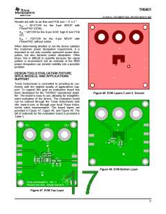
PowerPAD DESIGN CONSIDERATIONS
The THS4631 is available in a thermally-enhanced
PowerPAD family of packages. These packages are
constructed using a downset leadframe upon which
the die is mounted [see Figure 43 (a) and Figure 43
(b)]. This arrangement results in the lead frame being
exposed as a thermal pad on the underside of the
package [see Figure 43 (c)]. Because this thermal
pad has direct thermal contact with the die, excellent
thermal performance can be achieved by providing a
good thermal path away from the thermal pad
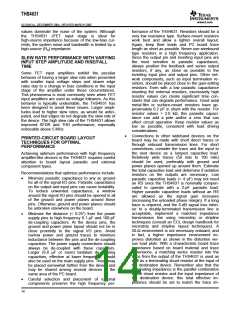
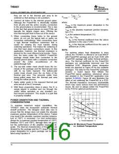
0.300
0.100
0.035
0.026
0.010
Pin 1
0.030
0.060
0.060
0.140
0.050
0.176
The PowerPAD package allows for both assembly
and thermal management in one manufacturing oper-
ation. During the surface-mount solder operation
(when the leads are being soldered), the thermal pad
can also be soldered to a copper area underneath the
package. Through the use of thermal paths within this
copper area, heat can be conducted away from the
package into either a ground plane or other heat
dissipating device.
0.035
0.080
0.010
vias
All Units in Inches
Top View
Figure 45. DDA PowerPAD PCB Etch and Via
Pattern
The PowerPAD package represents a breakthrough
in combining the small area and ease of assembly of
surface mount with the mechanical methods of
heatsinking.
PowerPAD PCB LAYOUT CONSIDERATIONS
1. PCB with a top side etch pattern is shown in
Figure 44 and Figure 45. There should be etch
for the leads and for the thermal pad.
DIE
2. Place the recommended number of holes in the
area of the thermal pad. These holes should be
10 mils in diameter. Keep them small so that
solder wicking through the holes is not a problem
during reflow.
Thermal
Pad
Side View (a)
DIE
End View (b)
Bottom View (c)
3. Additional vias may be placed anywhere along
the thermal plane outside of the thermal pad
area. This helps dissipate the heat generated by
the THS4631 IC. These additional vias may be
larger than the 10-mil diameter vias directly under
the thermal pad. They can be larger because
Figure 43. Views of Thermally Enhanced Package
Although there are many ways to properly heatsink
the PowerPAD package, the following steps illustrate
the recommended approach.
15

 TI [ TEXAS INSTRUMENTS ]