THS4631
www.ti.com
SLOS451A–DECEMBER 2004–REVISED MARCH 2005
2
4C
1
1
S
A
OL
) Ǹǒ Ǔ
Gain
)
p R GBP
p R GBP
p R GB P
F
F
F
−20 dB/
Decade
C
+
20 dB/Decade
Rate-of-Closure
F
2
(1)
Once the optimal feedback capacitor has been selec-
ted, the transimpedance bandwidth can be calculated
with Equation 2.
Noise Gain
GBP
GBP
F
+
Ǹ
20 dB/
Decade
*3dB
ǒ
Ǔ
2p RF CS ) CF
(2)
0
f
+
_
C
I(CM)
Zero
Pole
C
I(DIFF)
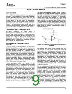
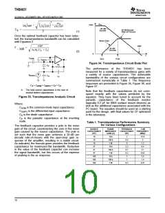
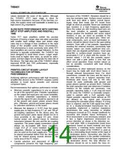
Figure 34. Transimpedance Circuit Bode Plot
R
C
F
C
P
The performance of the THS4631 has been
measured for a variety of transimpedance gains with
a variety of source capacitances. The achievable
bandwidths of the various circuit configurations are
summarized numerically in Table 1. The frequency
responses are presented in Figure 35, Figure 36, and
Figure 37.
I(
DIODE)
C
D
F
C
S
= C
+ C
+ C + C
I(DIFF) P D
I(CM)
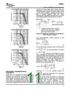
A. The total source capacitance is the sum of
several distinct capacitances.
Note that the feedback capacitances do not corre-
spond exactly with the values predicted by the
equation. They have been tuned to account for the
parasitic capacitance of the feedback resistor
(typically 0.2 pF for 0805 surface mount devices) as
well as the additional capacitance associated with the
PC board. The equation should be used as a starting
point for the design, with final values for CF optimized
in the laboratory.
Figure 33. Transimpedance Analysis Circuit
Where:
CI(CM) is the common-mode input capacitance.
CI(DIFF) is the differential input capacitance.
CD is the diode capacitance.
CP is the parasitic capacitance at the inverting
node.
Table 1. Transimpedance Performance Summary
for Various Configurations
The feedback capacitor provides a pole in the noise
gain of the circuit, counteracting the zero in the noise
gain caused by the source capacitance. The pole is
set such that the noise gain achieves a 20-dB per
decade rate-of-closure with the open-loop gain re-
sponse of the amplifier, resulting in a stable circuit.
As indicated, the formula given provides the feedback
capacitance for maximized flat bandwidth. Reduction
in the value of the feedback capacitor can increase
the signal bandwidth, but this occurs at the expense
of peaking in the ac response.
SOURCE
CAPACITANCE
(PF)
TRANS-
IMPEDANCE
GAIN (Ω)
FEEDBACK
CAPACITANCE
(PF)
-3 dB
FREQUENCY
(MHZ)
18
18
10 k
100 k
1 M
2
0.5
0
15.8
3
18
1.2
8.4
2.1
0.52
5.5
1.4
0.37
47
10 k
100 k
1 M
2.2
0.7
0.2
3
47
47
100
100
100
10 k
100 k
1 M
1
0.2
10

 TI [ TEXAS INSTRUMENTS ]