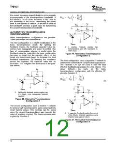
THS4631
www.ti.com
SLOS451A–DECEMBER 2004–REVISED MARCH 2005
T
T
A
they are not in the thermal pad area to be
soldered so that wicking is not a problem.
max
P
+
D max
q
JA
(9)
4. Connect all holes to the internal ground plane.
Although the PowerPAD is electrically isolated
from all pins and the active circuitry, connection
to the ground plane is recommended. This is due
to the fact that ground planes on most PCBs are
typically the targets copper area. Offering the
best thermal path heat to flow out of the device.
where:
PDmax is the maximum power dissipation in the
amplifier (W).
Tmax is the absolute maximum junction tempera-
ture (°C).
TA is the ambient temperature (°C).
5. When connecting these holes to the ground
plane, do not use the typical web or spoke via
connection methodology. Web connections have
a high thermal resistance connection that is
useful for slowing the heat transfer during
soldering operations. This makes the soldering of
vias that have plane connections easier. In this
application, however, low thermal resistance is
desired for the most efficient heat transfer. There-
fore, the holes under the THS4631 PowerPAD
package should make their connection to the
internal ground plane with a complete connection
around the entire circumference of the
plated-through hole.
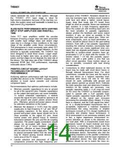
θJA = θJC + θCA
θJC is the thermal coefficient from the silicon
junctions to the case (°C/W).
θCA is the thermal coefficient from the case to
ambient air (°C/W).
NOTE:
For systems where heat dissipation is more
critical, the THS4631 is offered in an 8-pin MSOP
with PowerPAD package and an 8-pin SOIC with
PowerPAD package with better thermal perform-
ance. The thermal coefficient for the PowerPAD
packages are substantially improved over the
traditional SOIC. Maximum power dissipation
levels are depicted in Figure 46 for the available
packages. The data for the PowerPAD packages
6. The top-side solder mask should leave the ter-
minals of the package and the thermal pad area
with its via holes exposed. The bottom-side
solder mask should cover the via holes of the
thermal pad area. This prevents solder from
being pulled away from the thermal pad area
during the reflow process.
assume
a
board layout that follows the
PowerPAD layout guidelines referenced above
and detailed in the PowerPAD application note
number SLMA002. Figure 46 also illustrates the
effect of not soldering the PowerPAD to a PCB.
The thermal impedance increases substantially
which may cause serious heat and performance
issues. Be sure to always solder the PowerPAD
to the PCB for optimum performance.
7. Apply solder paste to the exposed thermal pad
area and all of the IC terminals.
8. With these preparatory steps in place, the IC is
simply placed in position and run through the
solder reflow operation as any standard sur-
face-mount component. This results in a part that
is properly installed.
4
T
J
= 125°C
3.5
3
θJ = 58.4°C/W
A
POWER DISSIPATION AND THERMAL
CONSIDERATIONS
2.5
2
θJ = 98°C/W
A
To maintain maximum output capabilities, the
THS4631 does not incorporate automatic thermal
shutoff protection. The designer must take care to
ensure that the design does not violate the absolute
maximum junction temperature of the device. Failure
may result if the absolute maximum junction tempera-
ture of 150°C is exceeded. For best performance,
design for a maximum junction temperature of 125°C.
Between 125°C and 150°C, damage does not occur,
but the performance of the amplifier begins to de-
grade. The thermal characteristics of the device are
dictated by the package and the PC board. Maximum
power dissipation for a given package can be calcu-
lated using Equation 9.
1.5
1
0.5
0
θJ = 158°C/W
A
−40
−20
0
20
40
60
80
100
T
A
− Free-Air Temperature − °C
Figure 46. Maximum Power Dissipation
vs. Ambient Temperature
16

 TI [ TEXAS INSTRUMENTS ]