PGA400-Q1
www.ti.com
SLDS186 –MARCH 2012
NOTE
Changes in the VDD voltage result in a proportional change in the output voltage because
the current reference for the DAC is derived from VDD.
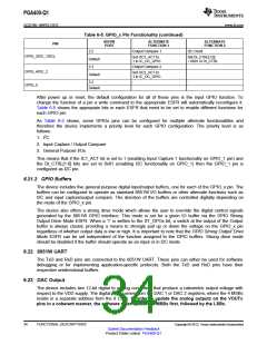
6.24 Input Capture and Output Compare
The device has two Input Capture and two Output Compare ports. Table 6-5 shows the GPIO pins of the
device that can be used for Input Capture and Output Compare ports. The capture and compare
functionality uses a 16-bit Free Running Timer for the events.
6.24.1 Free Running Timer
The Free Running Timer is a 16-bit timer that is different from the 8051W native timers. The resolution of
the Free Running Timer can be set to either 1µs/bit or 0.5µs/bit using 10_20_MHZ bit in Input
Capture/Output Compare Control Register (IC_OC_CTRL) in the ESFR memory spacer.
The current value of the Free Running Timer can be accessed using the Free Running Timer Shadow
Registers (FRTMSB & FRTLSB). This register in only updated upon request, it is not continuously
updated. When the IC_OC_TIM_LAT bit in the Input Capture/Output Compare Control Register
(IC_OC_CTRL) is set to logic 1, the current value of the Free Running Timer is written to the Free
Running Timer Shadow registers.
6.24.2 Input Capture
The device has 2 Input Capture ports. The Input Capture functionality can be enabled when the pin is
configured to be a GPIO by setting ICx_ACT (x = 1,2) bits in the Input Capture/Output Compare GPIO
Register (IC_OC_GPIO) in the ESFR memory space. When the user sets the corresponding bit to logic
high, the GPIO pin is configured for Input Capture functionality automatically.
The Input Capture port can be configured to either capture the Free Running Timer value on a rising edge
or falling edge using the ICx_EDGE bits in the Input Capture/Output Compare Control Register
(IC_OC_CTRL) in the ESFR memory space. Both IC_1 and IC_2 each have unique 16-bit timer capture
registers associated with them called Input Capture 1 Register and Input Capture 2 Register respectively.
When the corresponding rising or falling edge occurs the Input Capture peripheral transfers the value of
the Free Running Timer into the corresponding capture register and generates an interrupt to the 8051W.
6.24.3 Output Compare
The device has 2 Output Compare ports. The Output Compare functionality can be enabled when the pin
is configured to be a GPIO by setting OCx_ACT (x = 1,2) bits in the Input Capture/Output Compare GPIO
Register (IC_OC_GPIO) in the ESFR memory space.
The Output Compare port can be configured to either (1) Set the pin to High level when the match occurs
or (2) Set the pin to Low level when the match occurs. The user can configure the desired state of the
OC_1 and OC_2 pins at match using OC1_LVL and OC2_LVL bits in the Input Capture/Output Compare
Control Register (IC_OC_CTRL) .
Each Output Compare port has a unique 16-bit timer compare register associated with it. When the value
programmed in the compare register matches the value of the Free Running Timer, the Output Compare
peripheral changes the state of the corresponding pin to the configured value and generates a unique
interrupt to the 8051W. This occurs every time the value in the Compare register matches the value of the
Free Running Timer.
NOTE
For correct function of the output compare it is recommended that the MSB be updated first
and then the LSB.
Copyright © 2012, Texas Instruments Incorporated
FUNCTIONAL DESCRIPTIONS
35
Submit Documentation Feedback
Product Folder Link(s): PGA400-Q1

 TI [ TEXAS INSTRUMENTS ]