PGA400-Q1
SLDS186 –MARCH 2012
www.ti.com
Table 6-5. GPIO_x Pin Functionality (continued)
8051W
PORT
ALTERNATE
FUNCTION 1
ALTERNATE
FUNCTION 2
PIN
2.2
Output Compare 1
I2C Clock
GPIO_3/OC_1/SCL
Set OC1_ACT to
1 in IC_OC_GPIO
Set DI_CTRL[1:0]
= 0b01 in DI_CTRL
Default
2.3
Output Compare 2
GPIO_4/OC_2
GPIO_5
Set OC2_ACT to
1 in IC_OC_GPIO
Default
3.2
-
-
Default
After power up or reset, the default configuration for all of these pins is the input GPIO function. To
change the function of a pin a write command to the appropriate ESFR will automatically reconfigure it.
Table 6-5 shows the appropiate bits in each ESFR that need to be set to enable different functions for
each GPIO pin.
As Table 6-5 shows, some GPIOx pins can be configured for multiple alternate functionalities and
therefore the device implements a priority level for each GPIO configuration. The priority level is as
follows:
1. I2C
2. Input Capture / Output Compare
3. General Purpose I/Os
This means that if the IC1_ACT bit is set to 1 (enabling Input Capture 1 functionality on GPIO_1 pin) and
the DI_CTRL[1:0] bits are set to 0x01 (enabling I2C functionality on GPIO_1) then the GPIO_1 pin is
configured as I2C pin.
6.21.2 GPIO Buffers
The device includes five general purpose digital input/output buffers, one for each of the GPIO_x pin. The
buffers can be configured to operate as standard 8051W I/O buffers or other alternate functions such as
I2C and input capture/output compare. The direction of the buffers are controlled digitally depending on
the mode of the GPIO_x pin.
The device also offers a strong drive mode which allows the user to override the digital control signals
generated by the 8051W GPIO interface. This mode is set for a given IO buffer via the GPIO Strong
Output Drive Mode ESFR. When a ‘1’ is written to the ST_GPOx bit, a switch at the output of the Output
buffer is always closed, providing a means to strongly pull up or down the voltage on the GPIO_x pin
regardless of whether output data is low or high. It is important to note that the GPIO Strong Output Drive
Mode ESFR can be set independent of the function assigned to the GPIO buffers. Strong drive mode
should be disabled if the buffer should operate as an input or in I2C mode.
6.22 8051W UART
The TxD and RxD pins are connected to the 8051W UART. These pins can either be used for software
debugging or for implementing application-specific protocols. Both the TxD and RxD pins have their
respective unidirectional buffers.
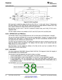
6.23 DAC Output
The device includes two 12-bit digital to analog converters that produce a ratiometric output voltage with
respect to the VDD supply. The digital input comes from the DAC 1 or DAC 2 registers, where the 4 MSBs
reside in a separate address from the 8 LSBs. In order to update the analog outputs on the VOUTx
pins in a coherent manner, the software must update the MSBs first, followed by the LSBs.
34
FUNCTIONAL DESCRIPTIONS
Copyright © 2012, Texas Instruments Incorporated
Submit Documentation Feedback
Product Folder Link(s): PGA400-Q1

 TI [ TEXAS INSTRUMENTS ]