PGA400-Q1
SLDS186 –MARCH 2012
www.ti.com
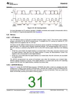
BANK_SEL[2:0]
IF_SEL
BANK0_EE_DATA[127:0]
EEPROM
Bank 0
EEPROM
(128-bits)
XRAMA[3:0]
PROGRAM
DATA_Out[127:0]
XRAMDO[7:0]
BANK1_EE_DATA[127:0]
I
8051
Microprocessor
n
t
E
E
P
R
O
M
EEPROM
Bank 1
Cache Read
Cache
Data_out[7:0]
EEPROM
e
r
Address[3:0]
(128-bits)
PROGRAM
EEPROM
DATA_Out[127:0]
Read
DATA_IN[127:0]
f
BANK2_EE_DATA[127:0]
a
c
e
EEPROM
Digital Interface
SPI
Cache
EEPROM
Bank 2
EEPROM
PROGRAM
B
a
n
k
DATA_Out[127:0]
EEPROM
DI_Address[3:0]
DI_Data_out[7:0]
(16 Bytes)
(128-bits)
PROGRAM
M
u
x
DATA_Out[127:0]
Cache Write
Data_In[7:0]
BANK3_EE_DATA[127:0]
I2C
S
e
l
EEPROM
Bank 3
EEPROM
(128-bits)
Cache Read
PROGRAM
Data_out[7:0]
e
c
t
DATA_Out[127:0]
OWI
BANK4_EE_DATA[127:0]
EEPROM
Bank 4
M
u
x
EEPROM
(128-bits)
PROGRAM
DATA_Out[127:0]
BANK5_EE_DATA[72:0]
EEPROM
Bank 5
EEPROM
(72-bits)
PROGRAM
DATA_Out[127:0]
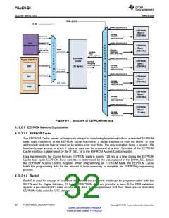
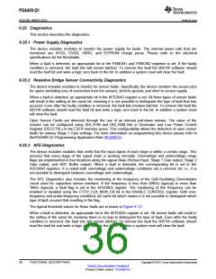
Figure 6-11. Structure of EEPROM Interface
6.20.2.1 EEPROM Memory Organization
6.20.2.1.1 EEPROM Cache
The EEPROM Cache serves as temporary storage of data being transferred to/from a selected EEPROM
bank. Data transferred to the EEPROM cache from either a digital interface or from the M8051 is byte
addressable and one byte at time can be written to or read from. The only exception being a special OWI
burst write/read access in which 8 bytes of data can be accessed at a time. Selection of the EEPROM
Cache interface is determined by the IF_SEL bit in the EEPROM Access Control register.
Data transferred to the Cache from an EEPROM bank is loaded 128-bits at a time during the EEPROM
Cache load cycle. EEPROM Bank selection is determined by the value placed in the BANK_SEL bits in
the EEPROM Access Control Register. When programming an EEPROM bank, the EEPROM Cache
holds the programming data for the amount of time necessary to complete the EEPROM programming
process.
6.20.2.1.2 Bank 0
Bank 0 is used for storage of customer data and is the only bank which can be programmed by both the
8051W and the Digital Interface. 16 bytes of EEPROM data are provided in bank 0. No CRC validation
against a pre-stored CRC value occurs when Bank 0 is programmed, and thus, there are no dedicated
EEPROM Cells used for CRC storage.
32
FUNCTIONAL DESCRIPTIONS
Copyright © 2012, Texas Instruments Incorporated
Submit Documentation Feedback
Product Folder Link(s): PGA400-Q1

 TI [ TEXAS INSTRUMENTS ]