PGA400-Q1
www.ti.com
SLDS186 –MARCH 2012
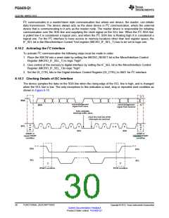
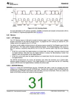
SDA
SCL
1 - 7
9
9
8
1 - 7
8
9
1 - 7
8
R/W
ADDRESS
ACK
DATA
ACK
DATA
START
condition
ACK
STOP
condition
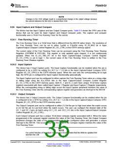
Figure 6-10. I2C Clocking Details
For more information on I2C protocol, operation, avaialble commands and example communication refer to
the PGA400-Q1 Programming Application Note (SLDA015).
6.20 Memory
6.20.1 OTP Memory
The OTP Memory space is 8 kB and is located at memory pages 3 and 4. This memory space contains
program instructions for the 8051W microprocessor. To program the OTP memory an external VP_OTP
voltage needs to be applied to the VP_OTP pin.
The device has the ability to lockout access to all memory spaces except the Test Register space from the
digital interface. This helps protect firmware intellectual property. The locking/unlocking of the access to
the OTP memory is achieved using 8051W Port 0 in the SFR memory space (P0[7:0]) in the following
way:
•
If P0(7:0) is set to 0xAA, the Digital Interface is in locked state. In this state, memories cannot be read
via Digital Interface. Note that once the Digital Interface is locked, the Micro/Interface Control Test
register is also not accessible via the Digital Interface.
•
If P0(7:0) is set to 0x00 while the Digital Interface is in locked state, then the memories are accessible
via Digital Interface.
The 8051W microprocessor can access all memories even when the memories are in locked state,
allowing software programs to execute. If the Digital Interface is in locked state and the CPU watchdog
causes a 8051W reset, the Digital Interface maintains the lockout state.
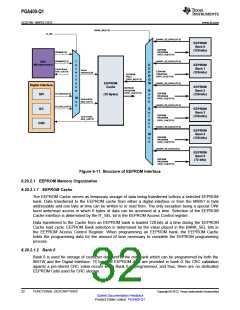
6.20.2 EEPROM Memory
Figure 6-11 shows the EEPROM Bank structure. EEPROM cells within a bank are activated only when
reading from or writing to their specific EEPROM bank. Therefore the contents of each EEPROM must be
transferred to the EEPROM Cache before reads and writes can occur to that bank. There are a total of six
banks of EEPROM, and they are located at memory page 5.
Copyright © 2012, Texas Instruments Incorporated
FUNCTIONAL DESCRIPTIONS
31
Submit Documentation Feedback
Product Folder Link(s): PGA400-Q1

 TI [ TEXAS INSTRUMENTS ]