PGA400-Q1
www.ti.com
SLDS186 –MARCH 2012
Due to limited number of erase/write cycles, the user has to keep track of the number of writes to
EEPROM Bank 0 and store the value inside the bank because it is the only bank that is accessable when
the write is occuring.
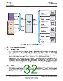
6.20.2.1.3 Banks 1-4
Banks 1–4 are used for storage of customer data. Each bank 1 through 4 provides 128-bits of data
storage for a total of 512 bits (64 bytes) of storage data. Since the 8051W does not have access to these
banks, only the digital interfaces can program them. Each time one of these banks is programmed a CRC
is calculated based upon the data held in the EEPROM Cache during program. This calculated CRC value
is stored internally and validated after bank programming is complete.
6.20.2.1.4 Bank 5
The firse 64-bits (8 bytes) of Bank 5 are provided to the customer for calibration value and/or general
storage. Byte 9 is used for the storage of the cummulative CRC values for banks 1-4 and the first half of
Bank 5. When programming Bank 5 it is required to place the cumulative CRC value for banks 1–5 in the
EEPROM Cache Address 0x558. This CRC value covers all data in banks 1 through 4 and the first 64-bits
of data in bank 5. Everytime programming of Bank 5 is completed the CRC value is validated. The
remaining 7 bytes of Bank 5 (0x559 - 0x55F) are not used.
6.20.3 RAM Memory
This memory space is used for 8051W scratchpad memory, such as intermediate calculation results. It is
a 256 byte memory space, and located at memory page 1.
6.20.4 SFR/ESFR Memory
The 8051W uses two types of memory storage, Special Function Registers (SFR) and External Special
Function Registers (ESFR). The SFR registers are used for 8051W internal operations, and cannot be
accessed external to the 8051W. The ESFR register exists on the same address space as the SFR,
however these registers can be accessed via the digital interface. The ESFR registers are used for
calibration, configuration, fault reporting and memory storage. The SFR/ESFR total memory space is 256
bytes, and they are located at memory page 2.
6.20.5 Test Register Memory
The test register memory space is used for diagnostic configuration, and testing for sensor calibration. The
test registers are located at memory page 0, and can only be accessed by the Digital Interface.
6.21 General Purpose Input Output (GPIO) Pins
The GPIO_x pins have multiple functions, including general purpose inputs/outputs (GPIO), input capture,
output compare or I2C. In the GPIO mode, the GPIO_x pins are connected directly to 8051W port pins.
The state of the pins can then be controlled through software by setting the appropriate I/O port SFRs in
the 8051W. Table 6-5 shows the mapping of the GPIO_x pins to specific 8051W ports.
6.21.1 Setting the GPIO Functions
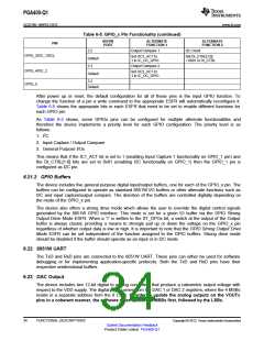
Table 6-5. GPIO_x Pin Functionality
8051W
PORT
ALTERNATE
FUNCTION 1
ALTERNATE
FUNCTION 2
PIN
2.0
Input Capture 1
I2C Data
GPIO_1/IC_1/SDA
Set IC1_ACT to 1
in IC_OC_GPIO
Set DI_CTRL[1:0]
= 0b01 in DI_CTRL
Default
2.1
Input Capture 2
-
GPIO_2/IC_2
Set IC2_ACT to 1
in IC_OC_GPIO
Default
Copyright © 2012, Texas Instruments Incorporated
FUNCTIONAL DESCRIPTIONS
33
Submit Documentation Feedback
Product Folder Link(s): PGA400-Q1

 TI [ TEXAS INSTRUMENTS ]