PGA400-Q1
SLDS186 –MARCH 2012
www.ti.com
I2C communicates in a master/slave style communication bus where one device, the master, can initiate
data transmission. The device always acts as the slave device in I2C communication, where the external
device that is communicating to it acts as the master node. The master device is responsible for initiating
communication over the SDA line and supplying the clock signal on the SCL line. When the I2C SDA line
is pulled low it is considered a logical zero, and when the I2C SDA line is floating high it is considered a
logical one. For the I2C interface to have access to memory locations other than test register space, the
IF_SEL bit in the Micro/Interface Control Test register (MICRO_IF_SEL_T) has to be set to logic one.
6.19.2 Activating the I2C Interface
To activate I2C communication the following steps must be made in order:
1. Place the 8051W into a reset state by setting the MICRO_RESET bit in the Micro/Interface Control
Register (MICRO_IF_SEL_T) to logic "high"
2. Give control of the memory to digital interface by setting the IF_SEL bit in the Micro/Interface Control
Register (MICRO_IF_SEL_T)to logic "high"
3. Set the DI_CTRL bits in the Digital Interface Control Register (DI_CTRL) to 0b01 for I2C interface
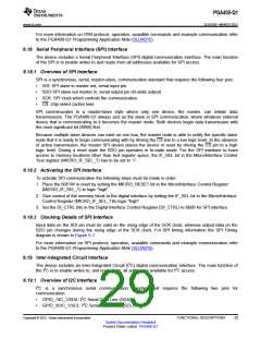
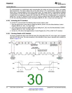
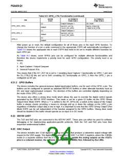
6.19.3 Clocking Details of I2C Interface
The device samples the data on the SDA line when the rising edge of the SCL line is high, and is changed
when the SCL line is low. The only exceptions to this indication a start, stop or repeated start condition as
shown in Figure 6-10
SDA
acknowledgement
acknowledgement
MSB
signal from slave
signal from receiver
byte complete,
interrupt within slave
clock line held low while
interrupts are serviced
Sr
or
P
S
SCL
1
2
7
8
9
1
2
3 - 8
9
or
Sr
SCK
SCK
START or
STOP or
repeated START
condition
repeat START
condition
SDA
SCL
SDA
SCL
START condition
STOP condition
30
FUNCTIONAL DESCRIPTIONS
Copyright © 2012, Texas Instruments Incorporated
Submit Documentation Feedback
Product Folder Link(s): PGA400-Q1

 TI [ TEXAS INSTRUMENTS ]